


 Visit the Project VGA Page


Entry 31
Progress #4
Posted on 2008/02/28 - 19:51Sorry to keep you all waiting. I've been busy. First, I had to wrap up the project for this semester for my university which resulted in the final version of the PID (dutch), the final design document (dutch), and a presentation (pdf printout, apple keynote, dutch again and 2+MB each). I also had to dig up the original requests (project outline and accompanying letter - all dutch) and finish up the hours spent on the project. I did a little live demo which took some effort (hooking up cables and such while in a presentation gave imho a really sloppy impression - so I decided not to do this at fosdem) but worked out all right and with that, this semester was officially over.
Then, I had to put together the FOSDEM presentation (pdf printout, apple keynote - english, 2+MB each) and after that all hell broke loose. People who were going to drive us to Belgium cancelled, so we didn't have a place to stay, meaning we had two days to get everything sorted out again. Try getting a hostel of some sort two days before an event which attracts about 4000 people and you just know you're in trouble. But anyway, Reinder ended up driving and Wouter Verhelst (thanks!) offered us a place to stay in his office. No showers or other luxuaries, but we didn't quite care anymore at this point. So, after that FOSDEM was a blast and saw & learned lots of new cool stuff about the linux graphics subsystems, and what other people are doing. People did end up a little disappointed that I didn't bring a machine to demo (I only had the card with me) and in retrospect I just worried to much and should've brought one. Oh well, to err is human I guess. On the other hand I ended up having some really interesting discussions about what other people would like to try out with this card and started thinking about the original plan of implementing full VGA support and continuing with full 2D support after that. Maybe that's not a good idea after all. But anyway, I'm getting ahead of myself.
With the new semester already started a couple of weeks ago (you've got to love this whole semi-overlapping system, while putting the final touches on one project you're supposed to start with the next, which is completely impossible in reality) I had some catching up to do, meaning the creation of a new accompanying letter and project outline, PID and design document (all dutch again). The last one isn't quite finished yet, I'm still working on it. For the people who take the time in reading it; you might notice they look an awful lot like the ones from the previous semester. That's just because the project looks an awful lot like last semester too. :)
Simultaneously I'm now following a class called interface technology, where they're trying to learn us new stuff about some PC interfaces. Better late than never I guess, but I have to do a presentation for that as well next week about, guess, PCI. The presentation pdf printout, apple keynote, dutch) walks through some of the history and basic layout of the bus. While putting this together I realised I made yet another error on the prototype; I never routed the Arbiter lines. This isn't a gigantic issue (the card will work) but it means it'll be impossible to do any sort of DMA with this card. That might be a little to slow for comfort, so the todo list for the next circuit board now looks like this;
- Fix power line for LM1086
- Fit config pins for JTAG / master serial selection
- Route M66 capacitor
- Route #REQ and #GNT lines
- Replace CPLD and VGA connector
I also want to do a proper logo on the final card which requires some final touches - it isn't quite finished yet. The M66 capacitor is probably optional but I want to add it anyway just in case somebody tries to clock the card at 66MHz and the motherboard refuses because a single capacitor is missing. It'll be tricky to do though, it's one of the most annoying spots on the board. The CPLD turns out to be pretty small (I knew it was small, but this might be too small for proper PCI support) so I'll replace it with the XC95288XL and the VGA connector I'm using at the moment doesn't have pins to keep the connector in place (and the board doesn't have spacing around the holes in the solder mask to solder any such pins) which makes plugging a VGA connector in or out really flaky. They're not really big deals but I'll have to find a proper replacement. Some other things I want to test before I call the board sem-final are;
- Test the memory
- Get some basic PCI working
- Do some multi-MHz clocking on certain signals
- Find out more about possible ESD considerations
Since I haven't cooked up a memory controller yet I'm still in the dark about whether or not the SDRAM is working. Same for PCI, the CPLD seems to be working fine but the moment I plug the card in a system it turns the entire computer in an overengineered power brick. This is probably because I'm not properly handling incoming PCI commands but I want to make sure there's nothing more fundamentally wrong with the card. Also, some EMI and power decoupling issues might arise when trying to clock the card at very high speeds, and I want to make sure everything can do at least a few dozen MHz without freezing up randomly. Finally, I'm clueless about how much ESD decoupling the VGA connnector requires. Officially it isn't a hotplugging interface but that doesn't stop 99% of the users of doing so occasionally.
Once I get above points out of the way (hopefully that won't take me another month) I made the suggestion at FOSDEM to produce a small batch of cards within about a month, so other people can start testing and working on the project. This, of course, with a big NO WARRANTY since it still isn't a fully verified consumer product but I know there are some people who'd really like to get started. This also helps us collect a little bit of feedback - if more people are doing EMI testing and such, we only get some really good hardware quicker. The costs for a single card (when doing a batch of 25) would be an 150 euro, if you want to join in get in touch with me. My email address can be found with some google-effort (comp.arch.fpga is a good start) or send a mail to the mailinglist. The moment we have 25 or more people I'll put some effort in arranging a batch to be assembled professionally. Please only contact me if you are sincerely interested.
Sorry again for the lack of updates here, cranking out 3 presentations and about 8 documents takes a little time. Hope you'll forgive me.
[: wacco :]
Entry 30
Main screen turn on!
Posted on 2008/02/09 - 22:28Next Monday I have to finish up a bunch of documentation for university about the card, Wednesday I've got to do a presentation with a demo, tommorow I'll be working all day somewhere else so in short; Argh! Busy! The XSVF parser still isn't working and I just can't seem to find the problem. The guys at comp.arch.fpga have been helpfull but still no results. Due to earlier mentioned deadlines however, I patched xc3sprog to work with the D2XX drivers (and let it recognise the CPLD) and gave that a go. Which worked, so there's nothing wrong with the hardware;
A little test app flashed in the FPGA
So at least I could continue testing the hardware for Wednesday. I grabbed the vhdl of Fabrice Derepas' site, adapted it to output data correctly for the DAC, added a little multiplier pattern for a bonus effect, mapped the pins and within the hour the DAC was also working correctly;
The DAC outputting to a screen
Somebody pointed out to me that I was missing a lot of red in that picture so since I made that quick movie I've changed the code somewhat so it'd produce some more red - it's really just the original squares again merged with the new pattern. I also got the question to throw the code online, so all three demo's (the CPLD one as well) are in this zip.
The revised output of the DAC
I'll be updating probably on Thursday or something with the revised code of the XSVF Parser and some cleaned up version of the patched xcs3prog. Sorry for the somewhat lousy quality of the movies and picture, I had to borrow somebody elses camera and it didn't seem to do what I wanted it to do. On a final note thanks goes out to Scanseer for giving me a free serial, I'll be giving that tool a testrun and a little review sometime soon when I've got the time.
[: wacco :]
Entry 29
JTAG XSVF Parser
Update 2008/01/31: Successfully flashed CPLD with test codeUpdate 2008/01/30: Couple of bug fixes
Posted on 2008/01/26 - 23:53
Let me start of by apologizing for the nearly two weeks of no updates. The kerneltrap interview generated a lot of new traffic (Hi!) but the timing wasn't so great, it's the end of the school semester meaning I've been studying like crazy for the last two weeks. A few exams, finishing up a bunch of applications and writing up a paper on network management in Ad-hoc environment. Fun subject if you have the time for it (if you're interested btw, grab it here) which unfortunately was absolutely not the case. But anyway I believe I've survived most of it and managed to hack together some stuff for project vga in the progress.
I've talked about the problems with open OCD getting to recognize my programmer correctly before and noted that it had some issues regarding parsing and playing XSVF files correctly. I was about to get into some serious retooling of open OCD when one of the developers said to another on the mailing list;
Also, taking into account the main purpose of OpenOCD (ARM debugging),
if statemove works with ARM cores, then everything is just fine.
I might be taking things a little out of context here but it's what motivated me to develop a custom XSVF parser for project vga. Since I'm using a standard FT2232D chip it should also work without too much effort on other programmers using this chip, which means Amontec JTAGkey programmers and the like. Right now though it's identifying the programmer by its location id, a specific string which is written in the EEPROM of the FTDI. This can be easily changed however. Because I had to understand what was going on in the first place I read up about JTAG and the FTDI commands to control the MPSSE controller. Note that I'm not using the JTAG libraries provided by FTDI but sending raw commands directly.
You can grab an early copy of the XSVF Parser here which should compile under cygwin on little endian machines. I haven't done any testing on anything else but windows yet, however I've been told that with the proper drivers and commenting the inclusion of the windows.h header it compiles on linux and after some slight changes it talks to an Amontec programmer as predicted. If you want to compile it get the latest FTDI drivers and libraries here (it's the closed source once, basically because they're quite a bit faster than the open source one I've been told - it shouldn't be too hard to support the open source one as well) and extract those files in the folder with the xsvfparser. Actual command line details are explained in the source file.
It isn't quite done yet since my main problem at the moment is getting the runtest to work properly. The documentation has a few things to say about runtest;
Defines the amount of time (in microseconds) the device
should sit in the Run-Test/Idle state after each visit to
the SDR state when the current XENDDR state is IDLE (see
the XENDDR command below). The initial XRUNTEST time is
zero microseconds.
Note: For XSVF containing XRUNTEST commands applied to
Xilinx FPGAs, the time parameter must be interpreted as
the minimum number of TCK pulses issued within the
Run-Test/Idle state after each visit to the SDR state.
Ok, fair enough, but the idea was that the parser didn't have to know about whatever was going on in the file or JTAG chain and that the XSVF contained all details. There's no way of knowing if we're supposed to clock or not. And if we assume all commands require clocking, will it cause problems on the CPLD? Both an FPGA and a CPLD are in the chain, so we have to find some middle ground. Obviously, since we're actually flashing data into the CPLD I favor not clocking since all commands I care about (that is, flashing data) are supposed to be for the CPLD. However, what am I supposed to do with the XCF? But wait, it gets even better, what does it say in the details regarding SDR commands?
If the TDO value does not match TDOExpected, perform
the exception-handling sequence described in the XC9500
programming algorithm section. [...]
If the last XRUNTEST time is zero, then go to XENDDR
state. Otherwise, go to the Run_Test/Idle state and wait
for the XRUNTEST time.
What exactly is this exception-handling sequence? I haven't found a clear description of it anywhere. Great. Also, the CPLD will obviously perform some kind of action during the period we're waiting, but we've already clocked out the data at this point. So in this scenario the TDO value will pretty much always not match what we're looking for the first time, which makes the exception-handling sequence even more important. Oh, and bonus points for the people who spot the contradiction. Is there a situation where we have to wait for the runtest time according to one description and not go to it according to the other? (hint: YES. And in that case, which state should we go to or stay in? I haven't got a clue)
So that's about it for where we are at this point. It can already execute correctly some easy files like fetching all device IDs which is more than openOCD could accomplish and gets pretty far with the somewhat more complex ones, but fails at properly implementing the runtest. In less than 3 weeks I'm having an audit about the project at my university so far, and the idea is to get at least something flashed into the devices by then. The week after that I'll be most likely presenting the prototype with some background info at FOSDEM in Brussels in the X.org devRoom. If you feel like dropping by, see you then!
Update 30 Jan:
I found out about xapp058 for
which is also some example code available
but alas, it only confuses more on certain points. I still haven't figured out what the exact byte (and bit) order
is in the XSVF files and everybody seems to just do something. The example code helps though. I do think I'm getting close;
tdoMask:	0x000003
tdoCache:	0x000008
tdoMatch:	0x000001
It looks like I'm just a few bits off, however, figuring out where the problem exists in the code is proving to be quite a challenge. Xapp058 has a few nice diagrams explaining the earlier runtest problem, but also introduces a new one; the first thing it does in Step 3 of Figure 9 (page 13) is shift out a single bit of data, without sampling TDO. I'm almost certain that this must be wrong; if I'd do that, the code would already fail when checking the device ID earlier. Also, the examples in xapp503 contradict this too. It's still suspicious though.
I uploaded the latest version of the parser (saved it over the old one, you can get it here) and it's a bit of a mess at this point due to all the debugging statements, so sorry about that. You can find the output here, when executing this xsvf which is supposed to do a blank check of the CPLD. A final note; I limited the number of xrepeats because it got annoying to see the same error 32 times. I periodically check if it might help to do it 32 times but so far it didn't matter at all.
Oh, and before I forget; xapp058 defines the XC9500 exception procedure so I implemented that as well. So far though it didn't really help mostly because maybe I'm still shifting in incorrect data somewhere somehow. I suspect this problem only showed up by now because this is the first statement where the data shifted in has different remaining bits from the first (or last) bytes that have to be shifted in. Or something like that. I'll keep on trying stuff out. I'm suspecting that the '8' I'm seeing is in fact my own bit I shifted in - meaning the CPLD is in bypass and not doing what it's supposed to do. Then again, maybe it's meant to be in bypass but should give a bit back as well, making the output '9'. That would fit the mask and explain some of the behaviour I saw when I was definitely shifting out incorrect bits. But it wouldn't explain why I'm shifting out that 1 bit in the first place. Argh.
Second update today
Found the culprit, I flushed the buffer when it was full, intended for when data was going to the Instructions
Register and the buffer size wasn't set yet (thus the default) it would flush and continue. There was an off-by-one
in there however causing it to flush the data early sometimes which under certain circumstances caused errors.
Really odd, but should do the trick now. This also means the code is probably bug-free enough to start programming
the CPLD with actual code! I'll continue tonight however with further testing and trying to get it to work for the
XCF as well, which needs some other things (like tck clocking in runtest) and seems to fail after the first bank is
tested. No idea yet why. See the error report here.
Update 31 Jan:
With some little effort getting familiar with ISE Webpack I wrote a little timer which counts up to some insanely
large number on every clock, which should result in a nice blinking LED roughly once a second. Turned out the
connection for the second LED connected to the CPLD is broken, something easily fixed if you have a soldering
station handy. Which I don't have right now. So two-led-magic will have to wait. The code used is here, the mapping
of the pins is here, and the reasons all PCI pins are already defined is because I've also been playing with
Ben Jackson's code but that part isn't working yet. Now, without further ado;
A little test app flashed in the CPLD
Exciting, isn't it? Unfortunately the system is unwilling to boot up with the card plugged in, I suspect it's because I'm not giving it some proper data when it's trying to initialise the card. The reason is that I've done some lengthy checking for shortcuts which might've been caused due to soldering the components on the board but couldn't find any. Haven't verified yet if all CPLD pins are actually connected to the wires, that might cause some corrupt data or something. But at least it should start the system up without using and registering my card, but it refuses. So sorting that out, as well as trying to get the XCF PROM programmed properly (still failing for reasons unknown - probably still a few bugs in the code) will keep me busy for the next days or so. On a final note, this is how the chain looks like in iMPACT, just to show you that I don't have to worry anywhere which device is being programmed or how my chain looks like (contrary to openOCD) because iMPACT takes care of those details;
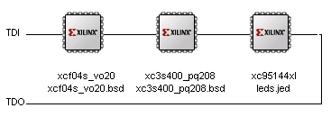
The device chain in iMPACT
[: wacco :]
Entry 28
JTAG Debugging
Update 2008/01/14: Some progress in supporting multiple devicesUpdate 2008/01/12: First succes with openocd added
Posted on 2008/01/12 - 19:46
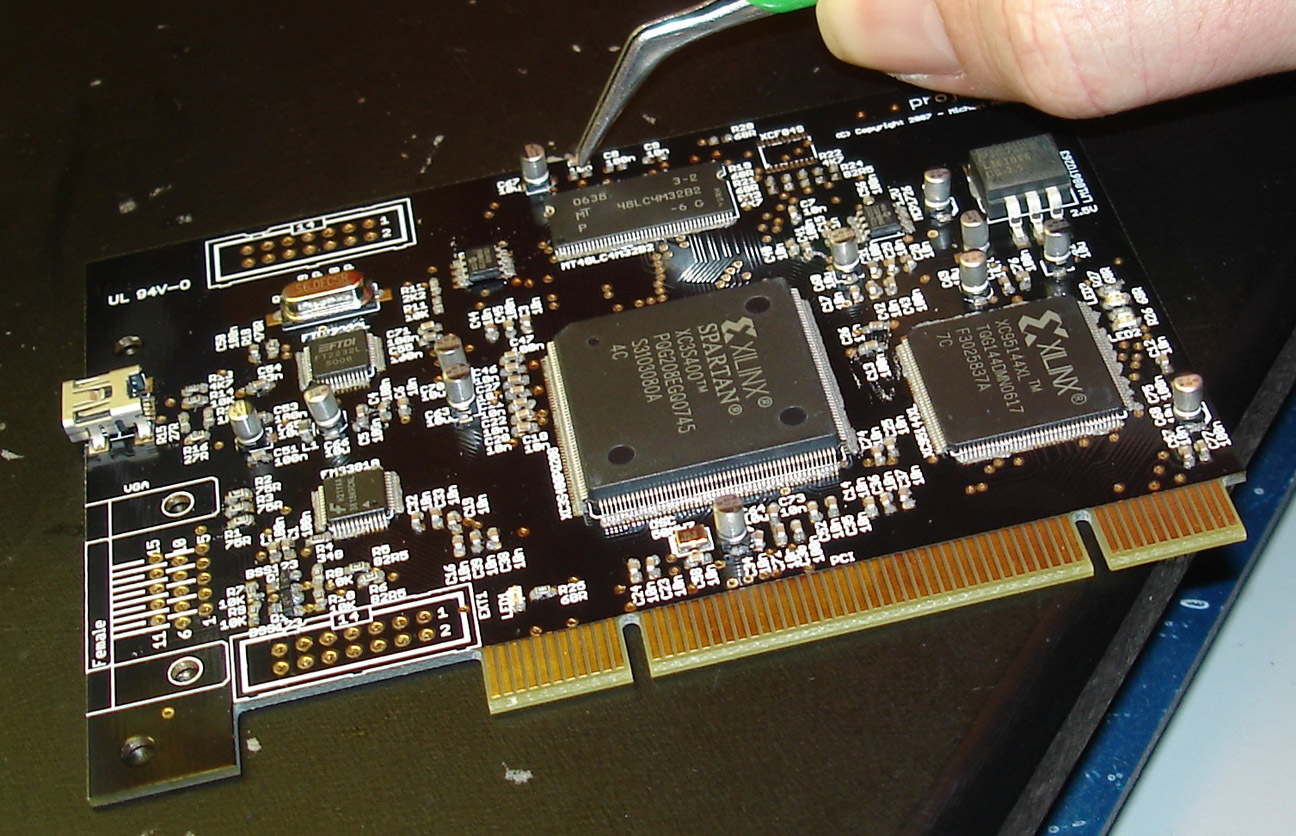
Well, it sure has been one hell of an exciting week. Soldering the first prototype together, getting rid of all solder shortcuts, making absolutely sure that it wouldn't go up in smoke, and then apply some power. It started up without a hitch and I got so excited that I tossed a single image on the frontpage, and continued working on the card instead of the website. Hope you'll pardon me, but four months 'in' the project and after countless hours seeing it come to life is amazing.
So the next step was obviously to get software figured out, installed, and running so I can actually start working on the HDL which needs to be flashed into the card. That turned out to be a bigger fight than I thought. First of all, I started up FTDIs tool called MPROG to flash some data into the eeprom of the ftdi chip to let it act as an Amontec JTAGkey. Turned out that figuring out what settings that where exactly took a while, but the end result was that the Amontec Demo tool could toggle JTAG commands on the bus. That implicitly also meant that the JTAG bus was actually working, so this was the first 'unofficial' confirmation that at least the PROM, the FPGA and the CPLD were working. After reading into how JTAG really worked on bitlevel (I somewhat hoped to avoid that, but found some good instructions in this document) I got the following data:
DR TDO: 0x5f046093 0141c093 49608093
That's three IDCODEs from the chips, albeit in a slightly mangled form (the first byte really reads 0xf5). The next step obviously was to try and do some more advanced stuff, so I prepared an SVF file with Xilinx iMPACT which would then be parsed by the Amontec svfplayer. However, it unfortunately turns out that my programmer differs too much from their original and the application crashed when trying to initialise. Too bad, we did some debugging but it seemed that we had to go for plan B after all, which is using openocd.
The problem with openocd is that it doesn't want to compile natively on windows. So after a lot of searching, asking for help on forums, and figuring out annoying error messages I got it to compile in cygwin. But oddly enough it still didn't want to connect with the ftdi drivers, so I ended up using the precompiled version from yagarto. For documentation purposes, here are some of the important bits of the configuration file;
interface ft2232
reset_config none

#jtag scan chain
#format L IRC IRCM IDCODE (Length, IR Capture, IR Capture Mask, IDCODE)
jtag_device 8 0x01 0x007 0xfe # xcf04s
jtag_device 6 0x01 0x003 0x09 # xc3s400
jtag_device 8 0x01 0x0e3 0xfe # xc95144xl
The interface is by use of an ft2232 (other details are filled in as well, but not interesting at the moment - see any other configuration file for those) but one without dedicated reset lines. I couldn't find confirmation that this is the proper way to indicate that, but it seems to work ok. Then, there are three jtag devices with their details which I grabbed from the BSDL files describing them. If I run openocd with this config it seems to be able to get all IDCODEs out of the devices correctly, but I'm not certain if it's using the configuration for that. It could be that it's using a 'trick' I used as well when doing it manually.
So anyway, openocd seems to be unable to parse standard svf files, but only accepts xsvf. xilinx has a little tool to translate from svf to xsvf (when exporting directly from iMPACT to xsvf it's using this as well) but it gives some very odd results. I'm not sure if it's the fault of openocd or xilinx, but when executed it gives errors like;
Warning: jtag.c:647 jtag_add_dr_scan(): scan data for a device in BYPASS
Warning: jtag.c:1132 jtag_read_buffer(): value captured during scan
didn't pass the requested check:
captured:    0x0349608093
check_value: 0x03d411824c
check_mask:  0x003ffffffc
I have absolutely no idea where that 0x03d411824c is coming from, but it doesn't make much sense. The captured value seems to be 0x03 with the first IDCODE (or last, depending on how you look at it - the one from the CPLD) attached to it. The other warning about reading from a device in BYPASS have I only seen once but doesn't sound too healthy either. So that's where we stand at the moment. If anybody has an idea as to how to get generated svf files into the xcf04s prom and the cpld or why this xsvf isn't working, please let me know. An other option would be to try and get xc3sprog working on a linux machine but that would require me setting up a completely new linux machine just for testing this tool, so I'm considering it a last resort.
Update 12 Jan:
I couldn't resist and continued fighting a bit while I should've gone to bed (I've got to work tomorrow morning)
but sometimes you just have an idea, and you have to try it out now. And it turns out I'm partially right.
Reinder decrypted the xsvf file and noticed that the numbers contained in it where shifted by a few bits, depending
on how far the device was in the chain. That made me thinking along the lines of; iMPACT knows what devices are in
the chain so it can compensate for it in the TDO checks, without wasting extra clock cycles, and openocd knows
how many devices are in the chain so will execute the commands in the xsvf file, making sure that everything
aligns. Which causes the TDO checks to be compensated twice. Which screws up things.
So what I did was make a chain in iMPACT with only the device I want to check (the CPLD, being the last in the chain, the device in question) and executing a command on it. Then, exporting it to xsvf and finally executing it in openocd. Et voila! The command was executed correctly, although some warnings still showed up.
Client:
> xsvf 0 xsvftest2.xsvf
XSVF file programmed successfully

Server: (a few times)
Warning: jtag.c:647 jtag_add_dr_scan(): scan data for a device in BYPASS
So that works. Brilliant. I can start hacking for the CPLD and if it turns out that all xsvf commands used by iMPACT are supported by openocd (which they are as far as I know) and can get the firmware flashed into the actual CPLD. If, however, I try to do it for the other devices (that being the fpga and prom) I'm still getting some weird data. I think it has something to do with the BYPASS warning, but I'll look at it tomorrow evening or something. I've been told that xcf proms are proprietary death traps, so we'll see how much hacking it'll require.
Update 14 Jan:
We're getting somewhere. After an upgrade to the latest version of Xilinx Webpack the "scan data for a device in
BYPASS" disappeared so that's one down, couple to go. When doing some more advanced things, I kept getting this
little bugger;
Error:   ft2232.c:477 ft2232_add_pathmove():
BUG: rti -> tlr isn't a valid TAP transition
After some fighting, I got openocd compiling correctly. The trick is to use the 'make' command that actually comes with cygwin, not the one from whatever tool that's installed on my computer as well, causing me to think I'm using the correct make when in fact I'm not. D'oh. Right now I'm compiling it with;
./configure --enable-parport --enable-ft2232-ftd2xx
--enable-amtjtagaccel -with-ftd2xx=/cygdrive/c/CDM/
Be careful with that last directory listing. The latest drivers from ftdi come with an amd64 and i386 folder, so make sure you copy the library from the correct folder into the folder below it, and give that folder to configure since that folder also holds some other files that you'll need later when compiling (an header file in particular).
But anyway, back to that transition error. xapp503 reads at the bottom of page 21 that "If the state is 0x00 (Test-Logic-Reset), then force the TAP to the Test-Logic-Reset state via the guaranteed TAP reset sequence: hold TMS High and apply a minimum of five TCK cycles. For non-zero state values, if the TAP is already in the specified state, then do nothing. Otherwise, transition the TAP to the next specified state." In other words, it warns us that it'll give odd XSTATE commands, and openocd starts throwing up when it sees them. I took the liberty of trying to fix it since I'm considering it a bug, and changed line 473 of ft2232.c to;
else if (tap_transitions[cur_state].high == cmd->path[state_count]
|| !cmd->path[state_count])
	buf_set_u32(&tms_byte, bit_count++, 1, 0x1);
I added the second condition, since cmd->path[state_count] is 0 when we're supposed to go to TLR. When that happens, output a at least a clock with tms high, until we've resetted stuff. I'm not sure if this is completely correct but at the moment things seem to work;
> xsvf plain test3.xsvf
XSVF file programmed successfully
That leaves a couple of other issues, like the fact that I still can't get any valid data in or out of the xcf except when it's not supposed to give any data. Reinder suspects that the other devices aren't being properly put in BYPASS, we'll have to look at it. Also some more complex statements seem to screw up openocd so we've still got some work to do before we can start flashing HDL stuff into it.
[: wacco :]
Entry 27
Card assembly
Update 2008/01/08: Finished assembly prototypeUpdate 2008/01/07: Work in progress picture added
Posted on 2008/01/05 - 13:03
The circuit boards arrived yesterday! Four days early! They all appear to be in perfect order, except for two little cosmetic issues on one of them. Since I only have components for two cards anyway and am now the owner of three circuit boards, this one will be used last, if ever, as a prototype. Enough talking, time for pictures!
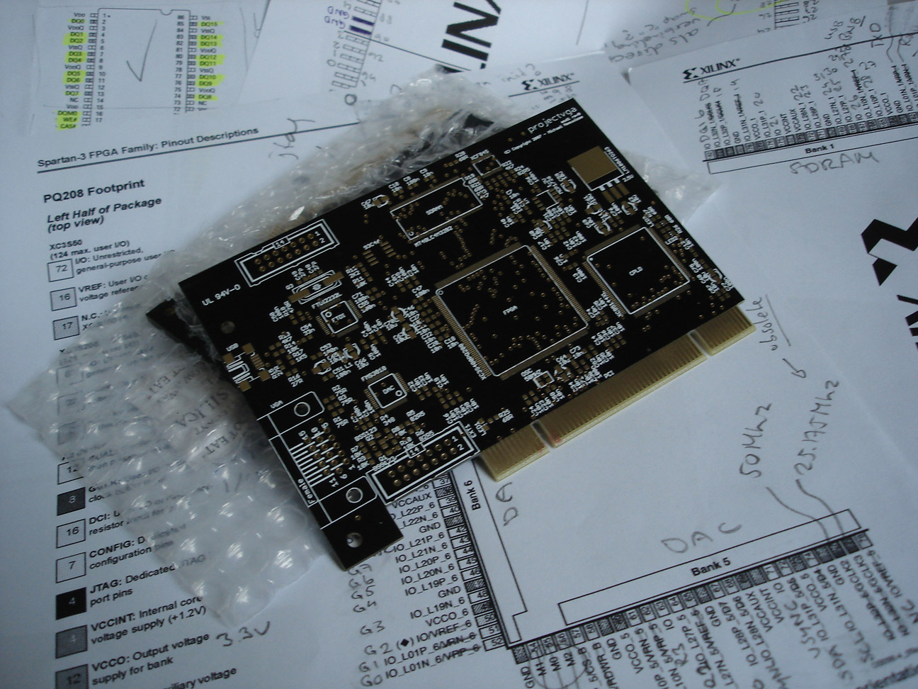
Pictures by Stefan
That last picture is just a little bonus to give you an idea of how I planned the FPGA IO, which is used as a background for some of these pictures. The black finish makes it really hard to get the wires showing on a photo so Stefan had to play a bit with the light to give you an idea of how it looks. I'm extremely happy with how they turned out.
Some details
On the left you can see a little green dot on top of the lower two data signals going to the extension connector. I'm not sure what it is, but it's not supposed to be there and it's stuck. You can see that the solder mask didn't attach to the board there, and the wires have gotten a little solder finish. Luckily, there's no shortcut between the two wires and even if it did it's "only" the extension connector that wouldn't work. It does make me paranoid enough however to not use this board. It also has a little spot somewhere else where it looks like the solder mask didn't fully attach to the board either, but it's in the middle of a ground plane so it doesn't matter.
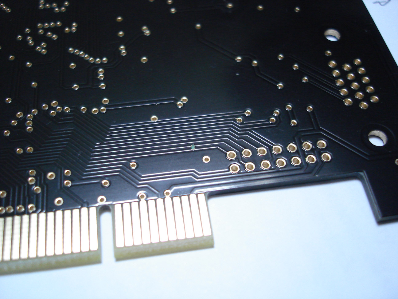
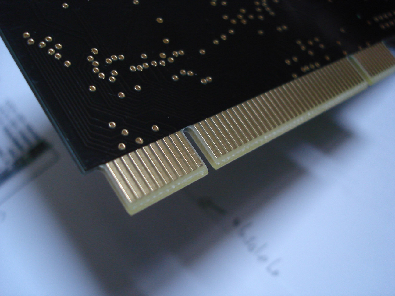
On the right you see the finish of the PCI connector. Although I didn't give PCBcart explicit instructions they figured it was in fact a PCI connector and made the cutouts round (although that might've been because their CNC machine couldn't get a straight cut there) which is perfect, and also trimmed the end of the connector a bit giving it a V shape, so you can really plug it in a connector.
Next monday Reinder and me will be (if all planning goes well) putting the first card together, so more pictures will follow then on this page.
Update 7 Jan:
Didn't finish today, we we're almost there but the lab at university closed for the night, so we had to leave. The
through hole connectors are still not placed, all the pins have to be tested before I'm even considering powering
it up since we were way to enthousiastic with the solder paste and I'm not sure we've fixed everything already and
the PCI bracket isn't finished yet (although that's really an optional thing). For your entertainment, a little
preview:
Reinder placing some capacitors
Update 8 Jan:
Well, between all the other stuff I had to do today I managed to get some work done on the prototype. I found a
couple of electrical shortcuts which we got rid of after some fighting with litze. To name a few; LED1, the USB
connector and the clk line of the DAC which where troubling. Hopefully they're all correct now. I find LED3 of
the FPGA suspicious since it wouldn't light up when I measured it for resistance, but that could be because the
meter wasn't providing enough current. Still, if the FPGA isn't able to get it lit either I'll have to replace it
since LED1 and LED2 would light up without a problem. I'll have to thank a couple of the guys from the E-tech lab
here for helping me out with some of the soldering work, it's not really my area of expertise and these guys did
an amazing job in virtually no-time.
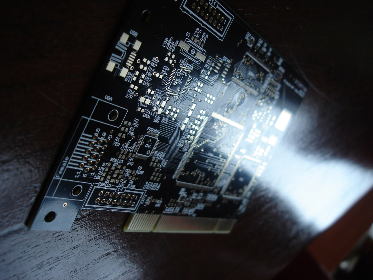
But anyway. All the connectors are now placed, all the components are soldered, and I'll be measuring like for the next day or so. I want to make absolutely sure that everything is correct before I power it up, which I haven't done yet. For all I know this card might be "DOA". In the design I already spotted two minor issues; First, the PCI pins TDI and TDO aren't connected. Although this is probably not a problem, it might prevent the system I'm going to plug it in from powering up. And second, there's no "AC connection" for the M66 pin on the PCI connector; I forgot to place a capacitor there. Again not really a big issue but it might make it impossible for the system to detect the prototype as a 66 MHz compatible card. We'll have to see. And now for your entertainment a bunch of pictures. Unfortunately the sun is already gone so I'll update these with better pictures tomorrow but didn't want to keep you waiting.
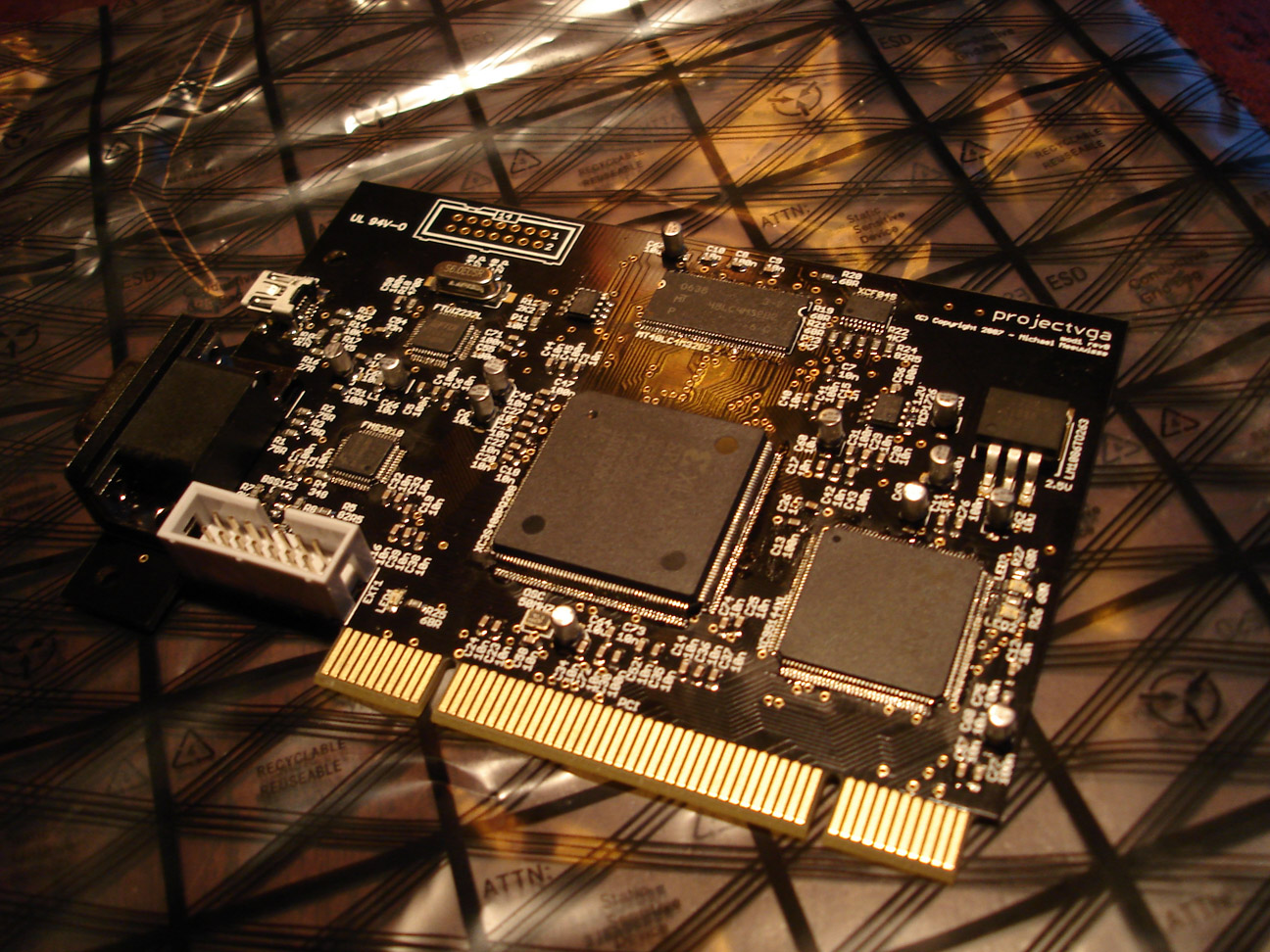


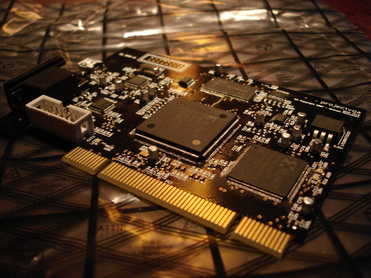
Finished assembly first prototype
On Thursday I'll hopefully be finishing the PCI bracket. In the mean time we'll have to do without. Thanks again to everybody who helped out here and there!
[: wacco :]
Entry 26
Finished Board art
Update 2008/01/02: Artist impression of board art addedPosted on 2007/12/23 - 14:55
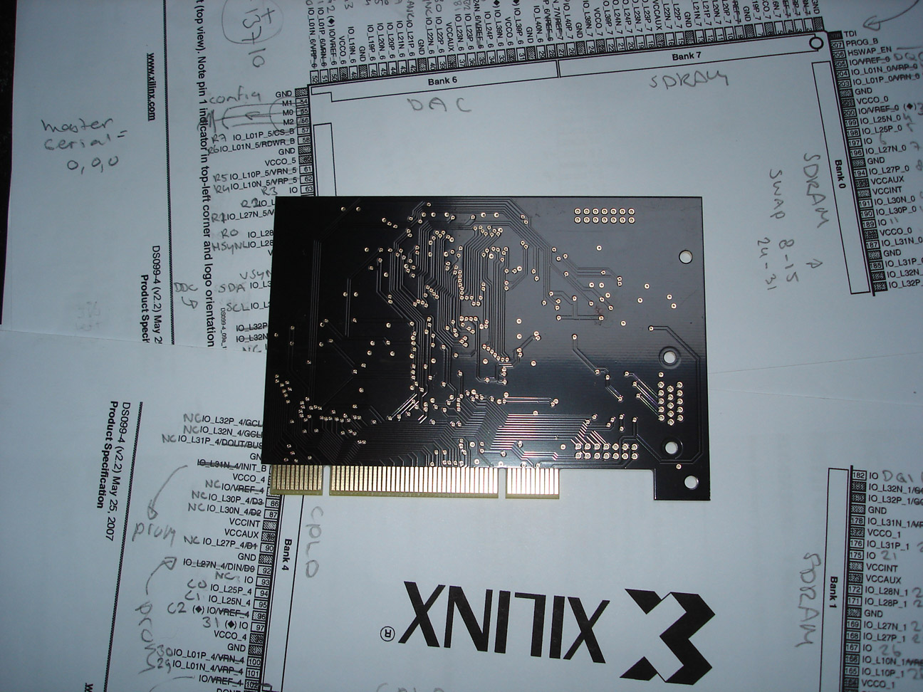
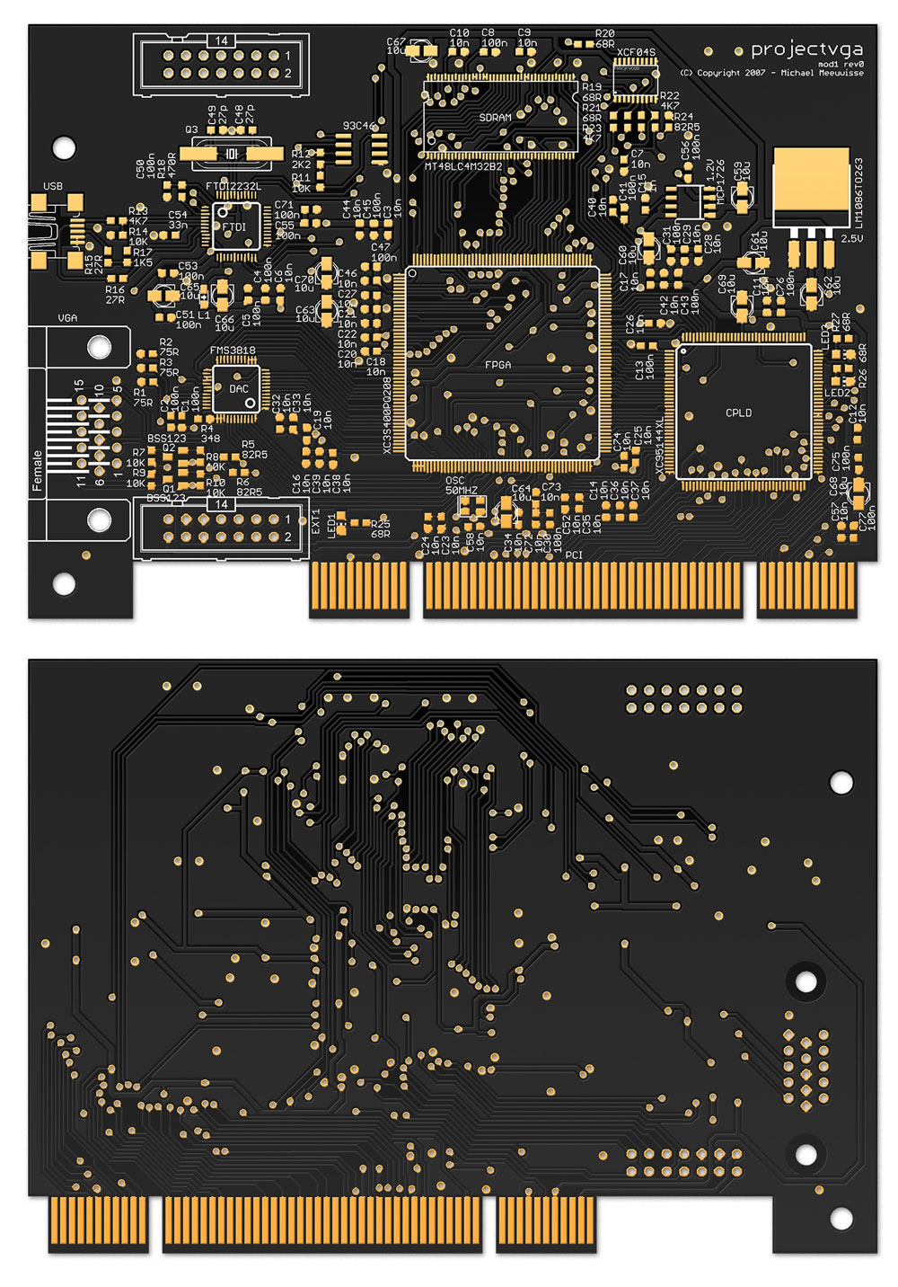
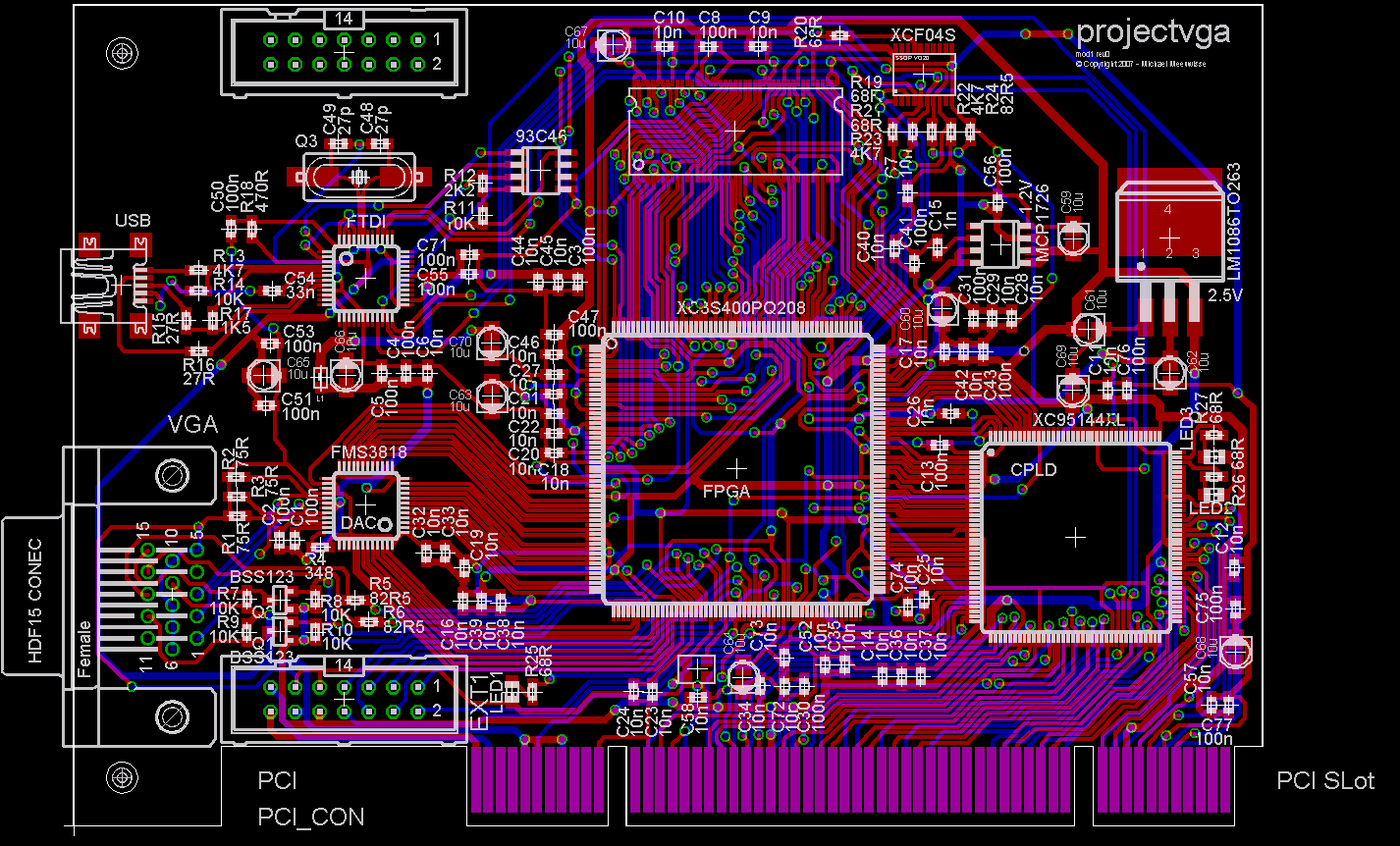
Two things today, first, some info about the finished circuit board art and second, the promised remaining part about the Module design. The part of the module design will be added in the previous post. I clocked in about 75 hours in about 7 days to get the board art finished because due to all kinds of other events related to this project kept delaying it. So I sat down on the 7th of December, started drawing, and gave myself the deadline of finishing it before or on the 14th. It's unbelievable how much work you can get done if you simply ignore everything else in life and I made the deadline, sorta. Over the following weekend I did some final adjusting and finetuning because there were some details I didn't like, but overal I tossed version 1.1 of the board art online to collect some feedback. Last week I did get just that, so I further changed the board to have 8 mil clearance everywhere, fixed some font issues, and other relatively minor things. You can grab version 1.2 right here. The finished board looks like this:

Board art v1.2
Another reason for this push is that it'll take about two weeks before I'll actually get the manufactured circuit board and my university will be closed for almost two weeks during the holidays. So instead of being unable to continue for a month I figured it'd be wise to let these two overlap, and I ordered a couple of circuit boards two days ago. I haven't slept for two days either because I'm a little excited about it, so it'll be an interesting two weeks. In case you wonder about the details:
PCBcart order 21 Dec 2007
Material:		FR4
Layers:			2
Board Size (width):	122.99 mm
Board Size (height):	86.04 mm
Quantity:		3 pcs
Thickness:		1.6 mm
Surface Finish:		ENIG -Electroless Nickle/Immersion Gold - RoHS
Copper Weight:		35 um
Min. Tracing/Spacing:	0.20 mm
Min. Annular Ring:	0.30 mm
Smallest Holes:		0.40 mm
Holes Numbers:		300 - 600
Surface Mount:		1 side
Soldermask:		Both Sides
Peelable Soldermask:	None
Soldermask Color:	Black
Matt Color:		None
Silkscreen Legend:	1 side
Silkscreen Legend Color:White
Gold Fingers:		116
Cutouts/Slots:		4
Testing:		Yes
Routing:		Individual
Lead Time:		in 15 days

File:			Version 1.2
Unit price		€ 14,91
Quantity		3
Tooling cost		€ 42,06
Total			€ 86,78
Shipping cost		€ 16,38 (DHL)
Total			€ 103,16
That's actually very cheap for some prototype circuit boards. I figured that if I were to do this project, I might as well make it look nice, so I ordered them at PCBcart which has the possibility for 'hard gold' PCI fingers, manages the cutouts for me, can do a black finish of the soldermask and actually accepts Eagle files straight away - no worrying about gerber files. Pretty much everybody seems to have a good experience with them so I didn't mind the slightly higher cost. I prefer to have perfectly working boards than a few bucks cheaper, and not being sure if everything is correct. But even with all those features they're still far cheaper than any other shop I asked, so if the boards turn out to be correct other companies will have a hard time convincing me to use their services instead.
A final thing I want to note about the circuit board is that I won't be having any PCI brackets for it. After some searching I matched the holes and distance of the connectors with these but getting just a handful of those with the correct holes punched in them would cost me a small fortune. I might try to produce two or three of them by hand at my university, but if that won't work the prototype will simply have to do without a bracket.
Update 2 Jan:
madwizard was kind enough
to do some photoshop magic and render a very nice version of the circuit board art, which hopefully gets close to
how the end result will look like. Enjoy:
Board art v1.2 - Photoshop rendering by madwizard
Happy holidays & Happy Newyear!
[: wacco :]
Entry 25
Progress #3
Update 2007/12/13: Early release board artUpdate 2007/12/10: Added talk about fpga<->cpld clock
Posted on 2007/12/07 - 17:15
It has been a hectic few weeks with all kinds of things happening. First, we had quite a few visitors (hi!) which killed the server I was lurking on, so I had to move in no-time. Which took all night. Then at some other point Reinder fixed a new server and we could move back to the old domain but in all this moving around we confused quite a few people so now there are multiple locations people can find us. Whatever. During all that I made some changes to the website to get the layout fixed up for more browsers, so it should work in pretty much anything that's capable of displaying text. And we've got a new, more permanent domain; projectvga.org.
Besides the whole polishing of the website I received lot's of mail and comments telling me this was a cool project and refering me to other projects, help, potential issues, you name it, I received it. And it's damn motivating so keep 'em coming, I love it. I was also asked to write an article for a magazine which will be distributed to a few thousand businesses to promote my university, and in return they will cough up some of the finance needed to cover the costs of the prototype. Great! All this did push back my planned deadlines though because simply 'finishing the circuit board' suddenly became 'find a spare hour'. That makes it all somewhat annoying, knowing that you spend a week doing only organisatorial stuff without getting anything 'constructive' done. Naturally I did get stuff done, but not the stuff I was planning to. So to get that out of my system I worked a bit on some new backend stuff for perennial last week. The idea I had isn't finished yet but is shaping up quite nicely, and I'll work out the details somewhere next year or something.
Anyway, yesterday the final components (the FPGAs) arrived, so I'm finishing up the circuit board. The north side of the FPGA and the power lines of the SDRAM still have to be worked out partially, but other than that most of it is done. There are a lot of 'rough edges' however so I'll spend probably most of next week finetuning it all. To give you an idea of what I mean with mostly done, a beta screenshot:
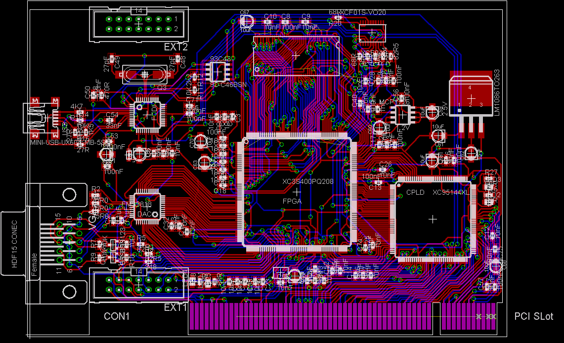
Current progress (click for large)
And I actually believe that's all for now. I added EXT2 for any extension cards, which could use some stability after being connected to EXT1. I'll probably keep all those pins unconnected, I *might* route some to the CPLD (just in case somebody says, "I wish you'd done that, then I could've done xyz") but I'm not sure if it's possible. In any case, hang in there, the next post will be the rest of the Modules design which I'll write up sometime soon.
Update 10 dec:
This is important enough to report straight away, but not big enough to create a new entry. I received an email
from André Pouliot and after a few mails he argued:
The clock in that case would use the general
routing inside the chip before connecting to the clock tree. That would
cause a lot of timing problem for the IO on the bridge side of the chip.
In some case you could see some pin captured before or after the
transition giving you erroneous data. Also since it would be using
general routing, after each rebuild the clock would have a different
delay before arriving to the flip-flop.
You can use any pin to output a clock. For receiving it you better use a
GCLK pin. I had once to do it without using a GCLK pin I can tell you it
wasn't fun.
He has an excellent point here, so I changed the schematic in such a way that there's now a signal from the CPLD going to GCLK2 on the FPGA. I took this opportunity to make the interface to the CPLD slightly larger, so I sacrified a LED on the FPGA for this and the bus to the CPLD is now 37 lines wide, with one dedicated clock line. I'll reflect this in the other documentation later. Unfortunately, the placing of the pins on both sides makes the clock line significantly longer than the other lines. But we'll have to deal with that somehow, I can't see any other way at this point.
Update 13 dec:
Again I don't feel like writing a full entry. I gave myself the deadline of friday to get the board art finished,
and although I've got one day left I'm mostly finished. I still got to fix some details to get the ground planes
rendered nicely, which is somewhat irreversible so you don't see them here yet. Other than that, I'm good as done!
Except for a final re-check to make absolutely sure that everything is in fact, correct. For your
entertainment:
Nearly finished! (click for large)
50+ hours so far just this week. I'm completely beat. This is definitely the last time I'm routing everything by hand. Next time I'll throw more layers at it until it can route it by itself. Or let some other idiot do it. Some changes you might not instantly spot are; PCI connector is now 3.3V compatible, has holes for a bracket, and gold plating is correct. All silkscreen text is now readable and ordered. Over 600 clearance errors (mostly because I turned the minimum clearance way up above what's needed) are removed. All power lines are now thicker. A bunch of capacitors for reducing noise have been relocated. Components and wires surrounding the clocks have been reorganised to reduce any noise, as well as the power lines near the DAC. And finally, a bunch of little changes for aesthetic reasons.
[: wacco :]
Entry 24
Module Design
Update 2007/12/28: Added module descriptions, changed talk about bus C.Posted on 2007/11/18 - 22:57
This is very much a work in progress. Feedback will be appreciated, nothing is definitive yet. This article will expand the moment more details are worked out.
Good news everyone! -- Hubert J. Farnsworth
After lenghty consideration I figured, what the hell, and switched to the GNU General Public License 3.0 so that should at least get a lot of those "You're not really Open Source!" smartasses out of the way. So there. I haven't checked everything yet so you might find BY-NC-SA still somewhere. Let me know if you spot it, I'll remove it at once.
I finally found the time to get accustomed to Inkscape, but only because it got about damn time that I figured out how to use graphics editor. So, if you haven't seen it yet, the talk about communication now has an accompanying Block Diagram to clarify a whole lot of things. This also gave me the possibility to sketch up some doodles I had laying on my desk for a while now, and worked out the module design for the FPGA and CPLD. After about a day work (I didn't say I got fast with inkscape) I ended up with this:
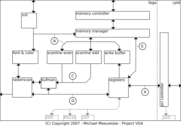
HDL Modules
So, right. I figure nobody really wants to read all of this right from the start, so I'll split it up in individual sections which discuss all the components. I'll make a note here that I won't quite discuss the gray areas partly because I haven't worked them out yet, and partly because they're available, but not really used. It's more for extentions, customizations and debugging that these ports are available in the first place. DDC is a notable exception, it's just that I won't really implement this at first. If a bus isn't discussed seperately check the module it's connected to.
A: Bridge bus
This is the bus between the FPGA and the CPLD, so it has some special properties. For one, it's limited to 38 lines
and that includes the clock signal. Second, being that it's a physical bus means it won't be as fast as everything
else and will probably need some extra buffering. Part of the PCI Controllers' job is to remap the memory space and
IO space, so this means there won't be 32 address lines needed. The other bits might be useful for Bus Command
singals, however because these are also used as Byte Enable during the data phase of the PCI spec, this might not
entirely be possible. Currently it might be possible to have AD[31:0] and C/BE[2:0], CLK, IRDY and TRDY. In this
setup, a subset of C/BE[3:0] will be mapped because not all options will have to be implemented by the FPGA. For
example, IO and Memory Read/Write can use an address line to indicate what space is used. Frame will be mapped
to IRDY meaning the FPGA will always have to be ready for recevining, which isn't unrealistic. With TRDY the FPGA
can let the CPLD know it wants to send data, which can then be acknowledged somehow. Lines like IDSEL can be left
out since the bus will no longer be shared among devices. In any case, 38 lines will be tricky but not impossible.
B: Memory bus
The memory bus connects the buffers with the Memory Manager. It has a multiplexed address and data bus of 32 bits
wide. Control lines like device select are seperate for each buffer and driven by the Memory Manager. During the
init phase this bus is used and controlled by the Init module instead. It is bidirectional in the sense that data
can go from the buffers to the memory manager and vice versa, but each buffer individually can only be read from
or written to by the manager. There's no support for communication between buffers.
C: Cache bus
The cache bus is controlled by the Buffer Manager and provides the Raster Scanner with data. It's 32 bits wide
and can be used during retrace periods to put a new address value in a buffer. At all other times, depending on
a signal selecting a buffer, the bus contains valid data. This means that the retrace signal from the rasterscan
propagates to the buffers as an output enable signal. The buffers auto-advance their internal offsets, so no
control signal other than a clock is needed.
A discussion on the Open Graphics mailing list made clear that you don't actually need two buffers for this, since it's in hardware and all the buffers are dual ported. Also, there is already a rasterscanner which has a buffer manager embedded in it available. I'll have to read up on how it works exactly but it's probable that the buffer manager and two scanline buffers will be replaced by some simple glue logic and a single buffer instead.
D: Register bus
The register bus simply directs any register values which are requested or changed to the rasterscan in case they
relate to the mode settings. Fonts and colors are redirected to memory, which the Memory Manager then in turn
writes to the buffer if needed. Signals like when the Raster Scanner is in a retrace period are send to the
Register module. This bus will probably be only 8 bits wide, since the traditional DAC is programmed using 8 bit
registers. An few extra signals will indicate for which register the data is currently meant.
E: Direct-Read bus
This bus is here to make it possible to directly reply to PCI requests from memory. The registers module maps
incoming addresses directly to the Memory Manager using this bus and can signal the Memory Manager that it needs
this data in case the C/BE lines indicate so. The Memory Manager can then instantly send this request to the
Memory Controller which will return the data as fast as it can. This data then ends up on the Memory Bus (B) which
can be accessed by the Register module through this Direct-Read bus. Because the Memory Manager will be running
in a higher clock domain than the Register Module and PCI connection, it's possible to reply directly to read
requests. It should be possible to stay below the maximum of 16 clocks after a read started on the PCI bus (see
section 3.5.4.1. of the specification) with this setup. Writes are buffered, so a write immediately followed by
a read for the same address might cause a race condition. The registers module makes sure this won't happen.
PCI Controller
The PCI Controller listens in on the PCI bus and responds to requests specific for this card. This includes the
memory areas of the VGA standard if these are enabled in the appropiate register. If it detects a request it
replies and translates the address to a mapping. This in turn is then send to the Register module on the FPGA.
Similarly, if the FPGA wants to send something it let's the PCI Controller know which in turn sends this onwards.
Note that all requests except PCI related or address translation related registers are send onward to the Register
module. The only thing the PCI controller does is filter out the PCI details of the requests.
Registers
The Registers module is called this way due to lack of a better name. It receives requests from the PCI Controller
and sends these to the correct module if needed, or stores / retrieves any register that isn't specific to any
module in particular. For example, if the output clock is configured, this data is send to the Raster Scanner and
not actually stored in the Registers module. If a read request is performed this module uses bus E to interrupt
the Memory Manager and retrieve the data from bus B (not shown, considered part of bus E in the illustration). For
writes is places this data first in the Write buffer to support longer bursts. Reading is not possible as long as
there's data in the write buffer, the register will deny any requests.
Write Buffer
The write buffer is a dual ported fifo which makes it possible to receive write bursts from the PCI controller
without having to throttle or interrupt the memory manager. Nothing special here, although the memory manager has
to give it a fairly high priority - the registers module can't initiate read requests as long as there's data in
this fifo.
Memory Manager & Controller
The Memory Manager has to keep track of all fifos and requests, and prioritise accordingly. It can receive signals
from all fifos as soon as they have data to offer or request, and poll for the required address. It then passes
this address to the controller which communicates with the actual memory. The controller is given a handle for
each request which it will return with the data. The manager uses these handles to determine for which fifo the
data was originally destined and pass the data on correctly. The controller can temporarily pause the manager when
it's refreshing portions of the memory.
Init
The init module loads all configuration data like default fonts and the pci eprom in memory on startup. It talks
directly to the memory manager and can not be ignored by it. Only once the init module finishes loading, the
memory manager is allowed to start dealing with the other buffers. During this startup fase, the font & color
buffer has top priority, only after that the scanline buffers will be activated.
Scanline even & odd & Buffer Manager
These fifos manage the graphics data to be displayed. It's probably wiser to only implement a single fifo which,
due to it's dual port features, can be kept filled while the raster scanner reads from it. The buffer manager
issues the required addresses and can be configured by the registers module for other ranges. If we end up using
the OGP raster scanner, this is already done by the raster scanner instead and a buffer manager isn't necessary.
Raster Scanner
The raster scanner creates the correct synchronization signals for the vga output and reads from the scanline
buffers the visual data. If the scanner is currently in a text mode it does a translation to actual pixel data
with help from the font & color buffer. Finally, it sends this to the video output. The raster scanner can be
configured by the registers module for which mode it needs to be in.
Font & Color
The font & color buffer holds the font mapping and color palette for all modes requiring these. It can be updated
at any time by writes from the memory manager. The memory manager knows what section of the memory the buffer
duplicates and will send new data to the buffer if this part is updated. Because of this, the buffer doesn't hold
any address related data.
[: wacco :]
Entry 23
FAQ
Posted on 2007/11/12 - 01:29Last weekend there's been quite some traffic here with new visistors (Hi there! Hope you stick around!) and I saw a lot of people asking the same questions and/or making the same assumptions, so I figured I'd write down this frequently asked questions to clarify a few things.
200 Euros can't compete with an old ATI Radeon or card X
Correct. We're not. This is a development card meant to get development started on a usable platform, not
to be an end product as a video card. If you don't want to spend extra bucks for a true open source system
and you don't mind using closed source drivers under linux, and/or aren't interested in developing on programmable
hardware, don't bother with this card.
You'll never get it under 200 Euros, your components alone cost E158
I know that number is given on the parts list but note that this list has more
than enough parts for two cards. Components for one card are (roughly) E70. The moment we start making
more cards simultaneously, this price goes way down. However, the cards will still need to assembled on a circuit
board so there are additional costs (not mentioning packaging, administration, and whatnot) on top of this. That's
why the estimate is E200, we're really aiming for E150 but simply don't know if that's realistic.
Will it do 3D in the future?
A more informative roadmap of what our plans are is in the making, but for now I can't answer this. The reason is
that we're starting with basic VGA (your BIOS boot screen, and low resolutions like 640x480) and after that start
working on 'custom' driver development which will add 2D. We might do 3D, yes, but it all depends on how big the
community will grow who'll develop for this card, how far the OGP will get with 3D, and simply how much we can
cram in this card. If it won't, a possible version 2 of this card will.
I want to help!
Ok, I admit, it's not a Frequently Asked Question, but it popped up so I'm going to include it here anyway.
If you're not really of the tech-stuff, doesn't matter. Right now I'm looking for someone who's willing to do some
art work for example (you might've noticed that this site doesn't contain much diagrams and stuff) so if you're
a bit of a wizard with Gimp or photoshop, let me know. If you just want to donate money, I appreciate it, but I'm
not accepting any yet. Hopefully we can make a buck with this card and won't even have to accept donations, or if
we do, we might play it through the Open Hardware Foundation, if they're willing to help us out. All in all, if
you can donate time, drop a comment here with what your skills are (again, doesn't have to be technical!)
and I'll get back to you.
Update 11 Feb: I never seem to get around to actually contact people. Why won't you come join the party on our mailing list instead? You can subscribe, unsubscribe, or get help. Once you're subscribed you can send email messages to the list. Also, an rss feed is now available. See you there!
Getting a VGA signal is simple
Yes, a VGA compatible signal is relatively simple, but we're trying to implement the full VGA 'standard'. All the
screen modes like the mode you're in when the BIOS shows it's splash screen, and those 'old' 640x480 resolutions.
This includes a full VGA BIOS loaded during boot, which can then in turn be used by your PC BIOS, and all those
other nitty gritty system calls which you can do with 'int 10h'.
Your license isn't really 'Open Source'
This is now a non-issue after we've switched to the GNU General Public License v3.0. If
you still don't like this one, well, I don't know what will. :)
That's about it for now, I said there's been some traffic, not loads. If other common questions pop up I'll add them here. I'll add a progress update somewhere during the week.
[: wacco :]
Entry 22
Communication
Update 2007/11/15: Added block diagramPosted on 2007/10/31 - 01:26
As predicted I didn't do anything on the project last week and probably won't do anything this week either. All the other classes have a priority right now since the deadlines are 2nd (for one class) and 8th (for the other) of November. Fun. I also forgot to mention the updated schematic last time, get it here, or see the image below if you don't have Eagle. I've got two little issues remaining, one being that I don't know if I'll pull up or pull down HSWAP_EN (bank 0) of the FPGA, and pull up, down or float PWREN# of the FT2232.
Updated schematic
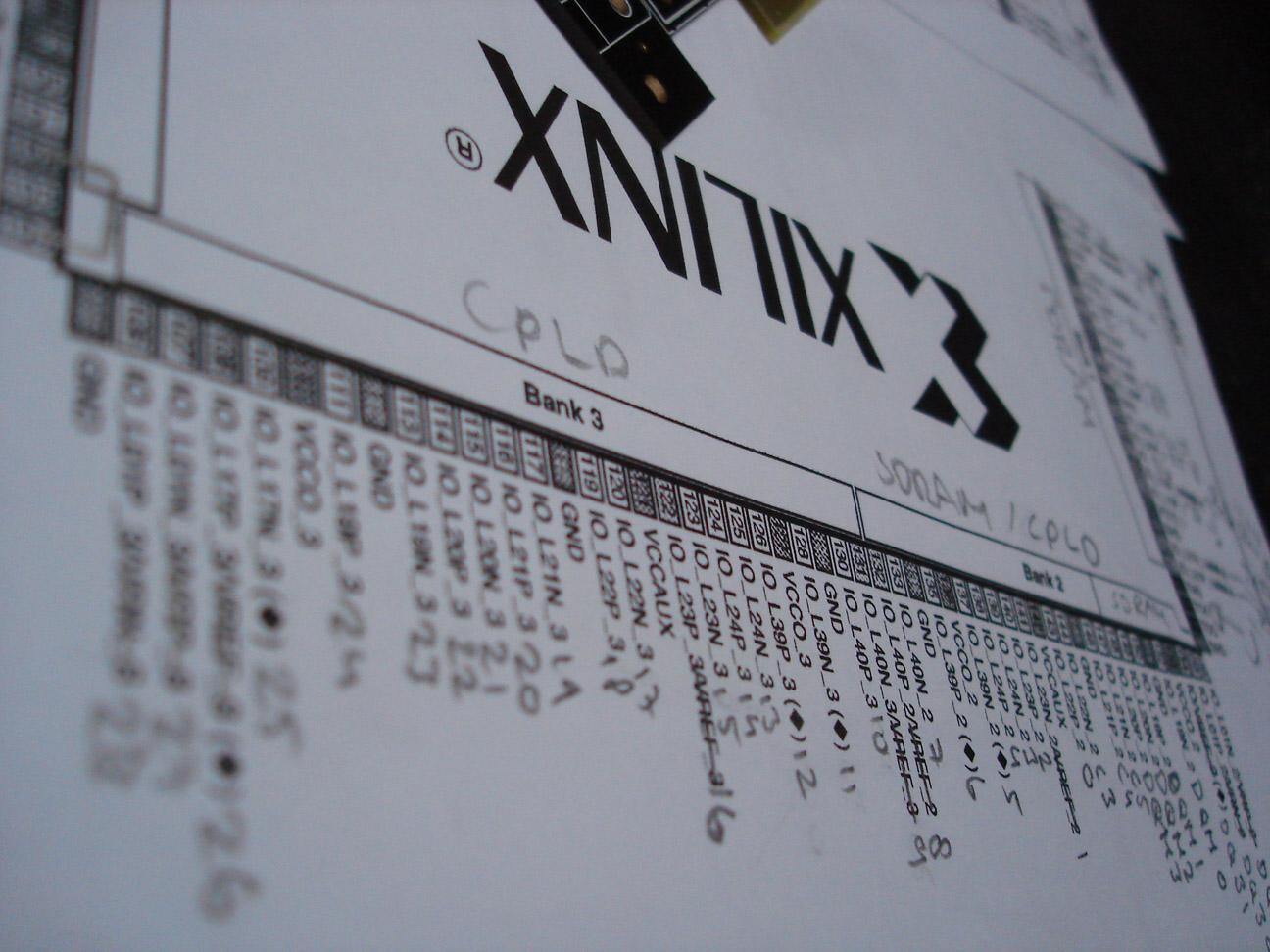
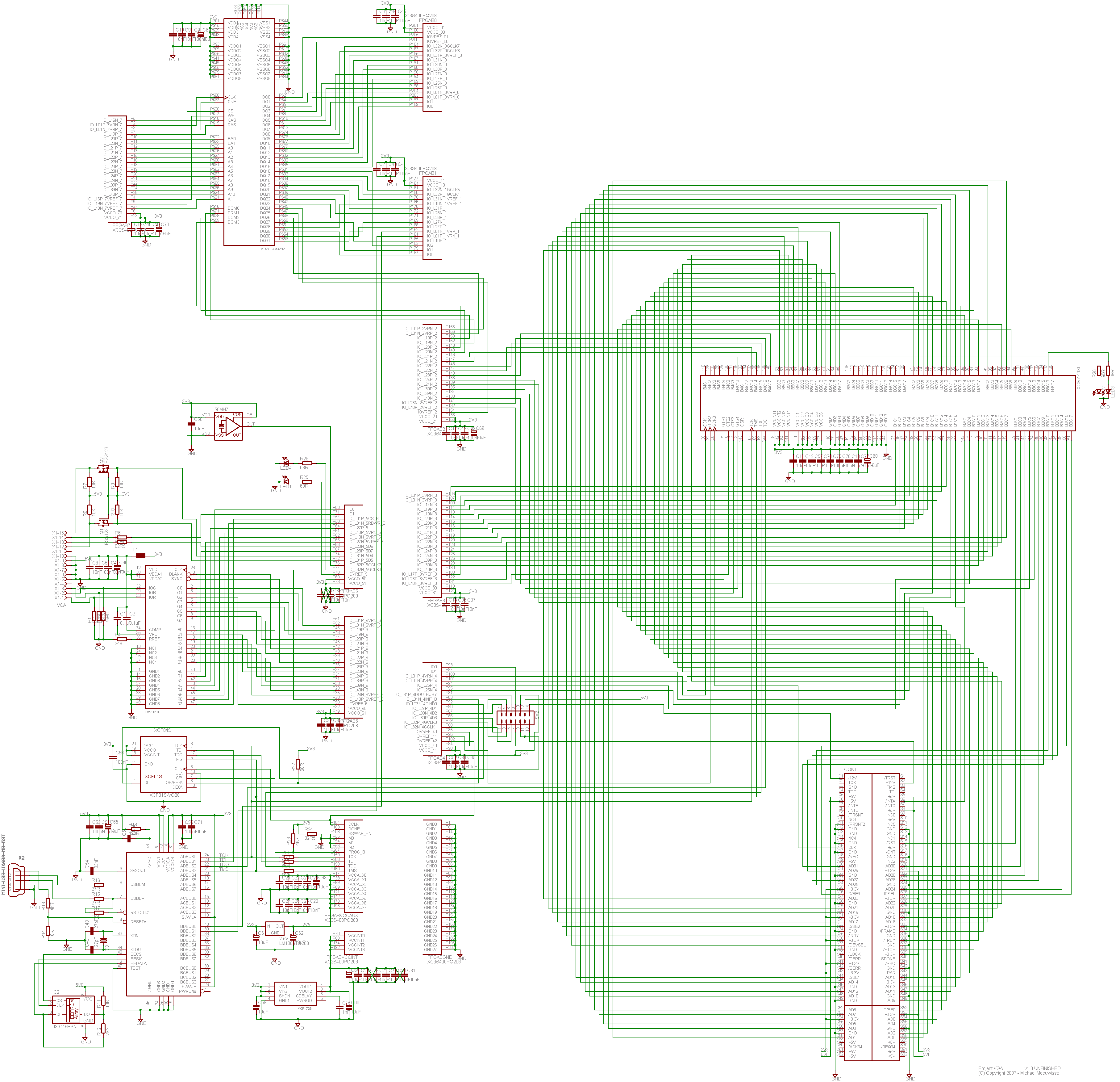
So anyway, communication. Quite a few points about the choice of components were already discussed in "Motivation #1" so I like to focus on the buses today. There are a few buses on the card of which most are fairly obvious and one is very roughly defined. While I'm at it I'll document which pins are used for what on the FPGA and CPLD. I've got it here on paper, but it's nicer to have it available online. The layout of the card is very straightforward so I didn't make an overview image. I'll leave that to your imagination. For all the exact pinouts of the chips, see their datasheets which I've listed here for your convenience. Be aware that they're all PDFs and could be a couple of Megabytes.
- PCI Specification 2.2 - Sorry, not going to give you that one due to copyright issues.
- FPGA: XC3S400 PQ208
- CPLD: XC95144XL TQ144
- SDRAM: MT48LC4M32B2
- DAC: FMS3818
- USB: FT2232D/L
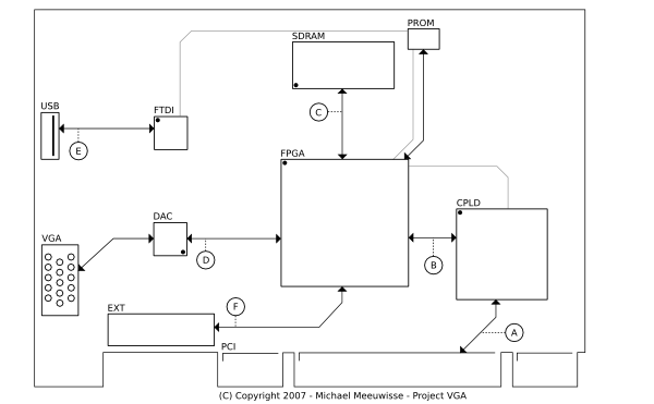
Block Diagram
A: PCI to CPLD
The card is designed to be 3.3V and 5V compatible and should be able to run on 33MHz and 66Mhz, although 66MHz
is very much dependend on how fast the CPLD can go with the code I'm going to write for it. Which means I don't
know yet if that'll work. Anyway, for 3.3V and 5V compatibility the CPLD needs to accept both voltage levels and
it does this out of the box as long as it's powered by a 3.3V supply. The clock is supplied by the PCI bus and
needs to be connected to a GCK pin on the CPLD. In this case, it ended up being GCK3 (pin 38). Then all the required
signals are connected to the right of this pin, except for INTA which I added at the last moment and is connected
to pin 35 of the CPLD. They are basically added in order, with the top and bottom side taking turns. That means
that RST is next on pin 39, AD31 on pin 40, etc. In order, you get; RST, AD[31:24], CBE3, IDSEL, AD[32:16], CBE2,
FRAME, IRDY, TRDY, DEVSEL, STOP, PAR, CBE1, AD[15:8], CBE0 and last but not least AD[7:0]. Naturally some dedicated
pins are in between but I left those out for clarity, if you count this out you end up with AD0 being pin 94. You
can see how this ends up in which function block / macrocell in the schematic, since I've made the eagle lib to
display that information. On the PCI connector only PRSNT2# is tied to ground, which configures the card as
consuming a maximum of 15 watt.
B: CPLD to FPGA
The other main connection of the CPLD is the databus to the FPGA. This databus is very broadly defined right now
because I simply don't know how much I'll be able to offload into the CPLD. The idea is that in the worst case
I can forward almost all signals to the FPGA, including the PCI clock. If, however, I'm going to do two clock
domains in the CPLD I've still got that option since GCK1 and GCK2 are connected to the FPGA. Also I don't know
if the GTS and GSR pins will be any use to me, so I made sure those are included. If I don't need them for their
special purpose I can always use them as general IO. The idea is that I have 6 'control' lines (including clock)
and 32 address/data lines. Not that I'll need them all as address (I can only access 16MB after all in the SDRAM)
so there might be some extra encoding there. In any case, how these pins will be used is somewhat unclear right
now and the only point of 38 lines is that it's pretty certain that this will be enough. The lines start above
the INTA line of the PCI connection and count all the way up until pin 135. I've declared the order to be C[0:2],
AD[31:0], C[3:5], but since GTS2,1,4,3,GSR is AD9,8,6,5,4 respectively this might change in the future. It's only
a naming convention anyway.
On the FPGA side of the story is most of bank 2, 3 and 4 dedicated to this connection. The SDRAM connection needed a few extra pins so the top of bank 2 is used for that, and bank 4 wasn't used entirely so the expansion connector sits there. But more about that one later. C5 is connected to IO_L21N_2, or pin 147, and everything else is a linear connection to the other side (skipping naturally the dedicated pins). A special note for pin 102 which is used for a clock to the EEPROM after configuration of the FPGA, and is skipped too for this connection. That makes the last pin, C0, end up on IO_L25P_4, or pin 94.
C: FPGA to SDRAM
The pinout of the SDRAM is somewhat odd in certain areas but I figured I could route them in such a way that it
makes mostly perfect sense for the FPGA. That's a contradiction, isn't it? In any case, the bus connects to bank
7, 0, 1 and a tiny bit of bank 2. The order of signals is the address lines A[11:0] starting at the bottom of bank
7, then all the control lines BA1, BA0 (which you could technically count as address lines, and probablly will be
used as such) followed by CS, RAS, CAS, WE, CKE, CLK. Here, the corner of the FPGA is reached so there's plenty
of room to get a good signal for CLK, and starting on bank 0 (pin 205) are the data lines DQ[0:15]. On bank 1 are
the lines DQ[16:28], and since the JTAG connection is at the end of this bank, two pins are used to create a
serial data connection to the B-bus of the USB controller. This can essentially be used as a 3.3V rs232
connection. However, due to these lines DQ[29:31] (not that they'd fit anyway on bank 1) are located at the
start of bank 2. Finally, DQM[0:3] are connected. These datamask lines will probably not be used, but might be
useful for something so are present anyway.
D: FPGA to DAC
The connection to the DAC is very simple since it's pinout makes a lot of sense. One side of the IC is dedicated
to the 'sensitive' signals and is directed to the VGA analog out. This side also contains the CLK signal which
therefore has to travel the furthest unfortunately. On the FPGA bank 5 and 6 are dedicated for this connection
so to make sure the CLK signal has enough routing space, this is connected at the top of bank 6 (pin 28). Right
after that the top of the DAC (it's upside down to get the analog side on the left) is connected. The order of
signals ends up being; CLK, B[7:0], SYNC, BLANK and G[7:0]. R[7:0] is located on bank 5 and after that the digital
VGA signal follow. HSYNC and VSYNC connect by means of a simple resistor, SDA and SCL go through a level shift
to get from the 3.3V FPGA IO at 5V DDC (an I2C bus) level. The last 3 pins of bank 5 are connected to the 50MHz
clock and two leds for whatever purpose. Can't hurt for debugging or general status indication.
E: USB to JTAG and JTAG chain
The JTAG chain is the order in which the JTAG compatible chips are connected. In our case, the data comes from the
A-bus of the FT2232, then goes to the FPGA PROM, followed by the FPGA and finally through the CPLD. The FPGA is
in there because JTAG has some other features than just in system programming which might come in handy. The
signal is 3.3V all the way, but because the FPGA wants to see 2.5V voltage levels there are some resistors added
to get that effect. I've copied this from figure 4 in xapp453.
The PROM comes before the FPGA because I wanted to copy figure 1 in xapp694
as much as possible, although it probably won't matter much anyway. All JTAG signals are dedicated signals on
the PROM, FPGA and CPLD so it shouldn't be a mystery where everything goes. On the FT2232 however I've copied the
pinout of this programmer (see the logical diagram) to make sure
that this would work. It's probably even possible to use their software if xilinx' tools turn out to be ineffective.
The PCI connector isn't in this chain because (rumor has it) a lot of consumer motherboards don't actually implement
these signals at all. If I'd take it up in the chain, I'd need some extra logic to detect this and only a few people
would be able to use it. Not worth the effort, thus left out.
F: FPGA to expansion connector
Right, after all these buses, I still had some pins left. The logic cells of the CPLD would be almost definately
be completely used up so the 80 or so data lines left there are a pity, but whatever. More interesting is that I've
got exactly 8 lines remaining at the bottom of the FPGA in bank 4. These lines (between pin 79 and 93) are
connected to an expansion connector for your entertainment. They're not buffered or anything, so don't hotplug
stuff on it or you might kill the FPGA. And they're 3.3V only! If you want to do anything with these pins, it's
your own responsibility. The full pinout of the connector (with pin 1 being top right, pin 2 bottom right, etc)
is as follows; pin 1 - 8 are data signals (see the schematic for exact names), pin 9 and 11 are ground, pin 10
is 3.3V, pin 12 is 5V, pin 13 is +12V and pin 14 is -12V. Be careful with these last two as they can only provide
little power; +12V max 500mA and -12V max 100mA.
Well, that's all for now. See ya later!
[: wacco :]
Entry 21
Progress #2
Posted on 2007/10/22 - 23:44Still no talk about the how, this 'week off' translated to close to 40 hours of work in just 4 days. So I was feeling like a trainwreck. The good news is that I put that much work in those few days because I was off for a little family holiday the rest of the week, which is also why this post is somewhat later. I'll try to do some things this week but I don't think much will happen due to other priorities I've got right now, like finishing some assignments for other classes and preparing for some tests that are coming up.
The schematic ended up getting a few final touches. Somebody mentioned that grounding all the remaining IO pins of the CPLD was a bad idea since an incorrect configuration could damange the CPLD this way. Better was to leave them unconnected and tie them high internally. I also dropped the second clock of 25.175Mhz. Although it seems important, I'm simply going to derive that (or at least 25MHz, which will also work without problems) from the 50MHz clock. Plus that IC was big and sitting in the way. Then, other voltages besides 3.3V were really appreciated on the extension connector, so I added all the power lines to it. Including -12V, which was a request and can be very handy for screens which need a contrast voltage. Finally I added a whole load of extra decoupling capacitors, found some properly sized electrolytic capacitors and added those, and changed all the packages of the resistors and capacitors to 0603. 0805 was non-stock for certain values I needed and so I had to use 0603 for some of them anyway.
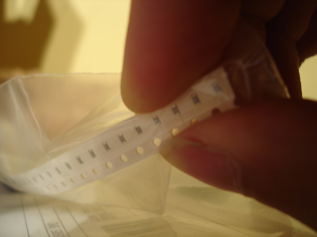
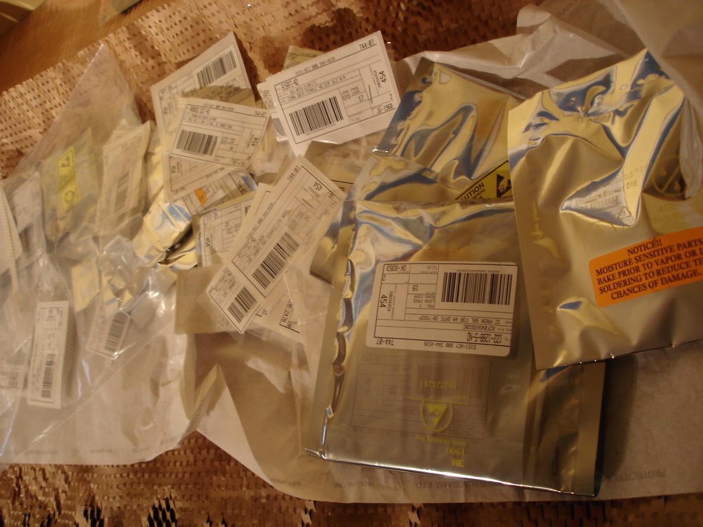
So yeah, Thursday I made a final Bill of materials and ordered everything at Digikey. Turns out the spartan 3 FPGA I want is now backordered. Damnit! There is a smaller (200k instead of 400k gates) one available but I wouldn't save that much so that would be a bad idea. So in the end I just ordered it and it'll be delivered somewhere in December. Not that much of a problem since most of the development can and will be done in a simulator first but it's annoying nonetheless. Everything else got delivered two days later! Brilliant! Turns out that 0603 for a size is really small. Note the tiny black dot on the white paper. That's a resistor.
Oh sh..!
Digikey order & parts list in detail
The rest of the week was spend completely on drawing the PCB which is, after pushing like crazy, still not finished. I'll hope to get to that point this week. I'm not going to release the brd file yet since I just know there are areas where wires get definately closer to eachother than 10 mil which will really end up incorrect. Also there are lots of power lines drawn as 10 mil lines, which is not going to work either. And the entire USB and JTAG area isn't drawn yet. Or drilling holes for a PCI bracket. Or the ground planes. And I haven't checked the solder mask and silk screen yet. Some art needs to be added, etc etc. There's still loads to do and I'm on it but I simply don't know when I'll have the time for it. I'm fairly sure it's not going to be this week.
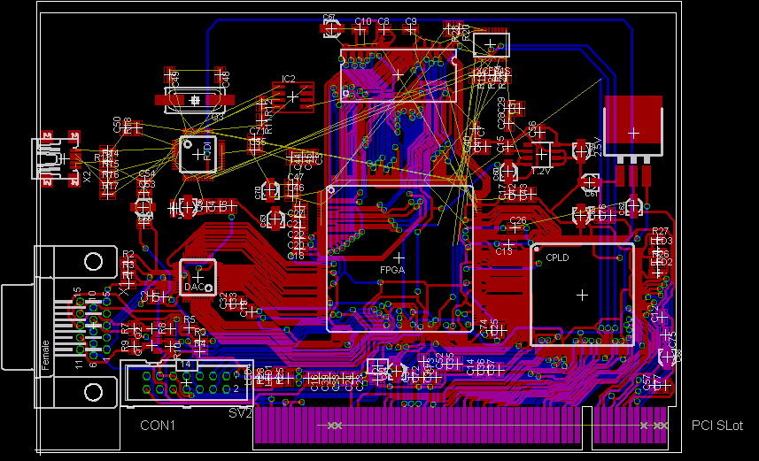
Unfinished! Mayhem!
It would've helped a lot if I placed all components a little higher on the board, but I was stupid enough to draw the SDRAM connection first and with that it was pretty much impossible to move the FPGA anymore. Unless I was going to draw it all over again, which I really didn't feel like. So yes, the board is pretty cramped. Anyhow, that's about it. I promise that next time will be about how everything communicates. Later!
[: wacco :]
Entry 20
Progress #1
Posted on 2007/10/13 - 14:06I wanted to talk a bunch about the how of the design, things like what databus lies where and connects what with whom, but I figured I can always tell you later since I've got more important stuff to rant about. Like, oh, I don't know, the nearly finished schematic maybe? Since last week I've made a heck of a lot of progress and I'll point out a few details which I think are interesting.
The first thing I want to note is the notion that VGA is a little outdated, and that I should implement a DVI connector. I've spend some time researching DVI and it has a few nice properties but chips supporting it is not one of them. The problem is that the digital DVI signals are a serially encoded with 8b/10b encoding and then send using current mode logic, combined referred to as TMDS. This stuff turns out to be pretty high speed and can't be done directly on the FPGA. I didn't really feel like including a dedicated chip which does a bunch of logical operations like the encoding scheme since it's a bit non-opensource like, but on the other hand it's not the biggest thing either. More importantly though, the only reasonably affordable chip (which is still expensive) I could find was the TI TFP410 and that one comes in a big package (not really the space for it), needs all data signals for the colors (not surprisingly) but doesn't implement the analog output. So I would still need the TMS3818 for this! I really didn't have space for both of them, including routing all the lines twice. Long story short; DVI is out. Maybe in a next revision.
Next, spare IO pins from the FPGA. I had 9 unconnected pins after I realised I'd forgotten to connect the DDC signals from the VGA connector. And I still wanted to connect the second RS232 connection from the FTDI chip to the FPGA. Not that I'd use it, but maybe somebody else would and it could always be handy for debugging purposes. A friend then mentioned that he'd love to see LVDS outputs on this board since a lot of laptop screens use those internally. That sounded really good since some kind of expansion port is always fun and opens the possibility for using this card for something else than 'just graphics'. But I didn't directly want to add a LVDS chip since that would limit the pins to out only, and maybe somebody wanted to use them for input as well. Plus I didn't really have the space nor time for it to route another chip on there. The idea of opensource is that other people can do whatever the heck they want with it (mostly, but definately for personal use) so if somebody wants the LVDS chip onboard, be my guest and make your own adaption. Or just make a little board that plugs right into the extra connector I've decided to include. It provides 3.3V, GND and 8 data lines. The connector uses a 2.540 mm pitch which is about as standard as it can be I believe. For the mathematicians among us, 8 data + 2 uart is indeed one pin short, so I dropped the second test led from the schematic. I hope you can all live with just one led connected to the FPGA.
Other stuff that happened is that I'm still not very familiar with Eagle. I wanted to use gEDA but I didn't feel like drawing all my needed components. Turns out a lot of them aren't in Eagle either so I still had to draw a bunch. I can only hope I did it right, otherwise chips won't actually fit on the circuit board. Another thing is that I didn't figure out how to draw busses (you have to use nets, not wires!) after I drew all wires by hand so a significant part of the schematic looks like this;

Oops, my bad
You can probably imagine that I didn't really feel like redrawing most of that with nets instead of wires. Just ignore it, I'll fix it someday when I have the time and it won't actually hurt anyone. More importantly are design choices where it turns out I'm not that familiar with electrical designs as I make people believe. For starters, I've never worked with ferrite beads before but it's recommended that the TMS3818 has one in it's power supply. Did I connect it correctly and is this a good choice? I wouldn't know. Also, the digital signals going in and out of the VGA connector are vague. The DDC signals are I2C, but I can't find anywhere if they really have to be 5V. In the end, I added a little voltage level switcher with a MOSFET on those lines. From other schematics I deducted that the hsync and vsync lines (which are only out, naturally) could be simply connected to a 3.3V chip with the addition of a resistor. But again, I'm not sure so help is always welcome here.
Does this make sense?
Lastly I have no idea how to decouple my power supplies for the FPGA, the CPLD and the SDRAM. I've found a helpful document from xilinx which explaines quite a few things and I've deducted by now that the capacitors I've drawn currently aren't going to be enough. So that needs work before I can start with the circuit board design. Oddly enough I was always taught at school that for decoupling you had to use electrolytic ones, but those are expensive, big and not used by anyone else. Even that document says that ceramic ones are best, which are the most sensitive for noise and might actually produce noise themselves. Weird, but hey, what do I know.
This needs work, since it won't work now
So all in all, I made some serious progress this week (at least, that's how it feels) and hopefully I can finish the board next week. Although I'm not to sure what thickness to use for what wires. If they're too thin, they break when etched and I can't use the circuit board, and if too thick I'll end up with inductance trouble. So yeah, next week will be a blast, even though apparantly I'm supposed to be a week off. Oh well. For everybody who wants to have a peek at the completed schematic, here's a PNG image. Or, if you have Eagle installed, here's a zip file with the schematic and my custom library. Feel free to check both for errors, I'd greatly appreciate it!
[: wacco :]
Entry 19
Motivation #1
Posted on 2007/10/05 - 17:15So, yeah, design and build an open graphics card. It was nice to see some people chime in on my last post, that doesn't seem to happen to often here. I want to start documenting some things here about this project so that people get a better idea of what and why I'm doing certain things with this card. I've got a document here in dutch filled with little notes to myself and links / page numbers to documents. See this post as a distilled version of the 'why' (and why not something else) I made certain design choises, I'll talk some other day about the 'how'.
But first I've got a little other issue I'd like to discuss. I have no idea how to call this project. I managed to cut through most of the red tape and got it approved as my university project for this semester, where it's now known as 'Project VGA'. On my harddrive it's in the folder 'ASNE' which means 'Advanced System and Network Engineering', which is the name of the general course I'm following this semester. Somebody already suggested "Wacco's Open VGA", and although that sounds catchy, it's a bit straightforward and 'WOV' doesn't sound 'cool'. If you get what I mean. So what I'm really asking is; if you have a cool idea for a name, and it's not in use or associated with anything else that might get me in trouble somehow, let me know! I'm probably going to route the circuit board next week and want to put some art on it with a catchy name. I'll do the art (got a good idea for that already) but I need a name ASAP.
Now that that's out of the way, back to the card. What I want to do is discuss some chips I'm going to put on the card and why I've chosen these. A big requirement for all these chips is that I can get my hands on them easily. This comes twofold, first I want everybody else to be able to copy me, and second I need to be able to buy them as well. I can't buy a reel of 2500 chips, I'm a student! Second, you should be able to get them from a general 'big' electronics shop. I'll be using digikey, so if they don't have it, I won't use it. Third, all components should be (albeit with some difficulty) capable of handsoldering. That's just to eliminate chips with Ball Grid Arrays on them, since if you don't have a compatible oven (I do have one at my university by the way) you can't use them. No-no on BGA and the like for home-soldering. Lastly, they need to be cheap. But I'm not going on a bargain hunt if I might save a few cents, I don't have the time on that (or else I'll end up spending 3 years in development).
Main FPGA: Xilinx Spartan 3 S400 (208 PQFP)
Right, the first and biggest chip! This is basically the biggest FPGA I could get which was still in a flat
package and isn't to overly expensive. Altera wasn't an option, since I couldn't get them easily, xilinx virtex
wasn't an option either because they have things like complete POWER cores onboard. Not that it isn't usable,
it's just not quite in the spirit of open source. If I'm going to include complete proprietary subsystems on the
FPGA and build my open source implementation on that, we're still stuck with these closed (you might be able to
get your hands on it, but not everyone can read and alter it) source components. So this was an easy choice.
Secondary CPLD: Xilinx XC95144XL-7 (144 TQFP)
The main problem with the FPGA is that it needs to be programmed before use. It can do this automatically, but
it'll probably take too long to respond to initial PCI commands. A CPLD doesn't have this problem, so a small
one is included between the FPGA and the PCI bus. Also, I've never played with these so it might be fun to simply
use it even if the FPGA is fast enough, and somebody already did this.
After some emails (thanks Ben!) I also found out that he reprogrammed the CPLD when the system was on (which had
some side-effects but nothing a reboot wouldn't solve) so no seperate power supply is needed, just tap straight
from the PCI bus. That somewhat motivated me to clone part of his design since this probably will work, and an
FPGA-only solution might not. Oh, and did I mention that the Open Graphics guys also have a similar setup?
Memory: 128Mbit SDRAM Micron MT48LC4M32B2P-6 (86 TSOP)
For memory I could use DDR material, but that would require a lot of pins on the FPGA side and other trickery
I'm not familiar with, and I was going to keep stuff simple! Even more simple than SDRAM would be SRAM since that
won't need a refresh cycle every once in a while, but that stuff is screaming expensive in larger quantities. So
it's going to be a simple SDRAM module. The FPGA has enough IO available so a 32bit bus wouldn't be a problem,
and this means we still get reasonably good performance on the maximum clock of 166MHz. I picked 128MBit since
it's big, but not expensive-big. It'll be plenty for now.
DAC: Fairchild FMS3818 (48 LQFP)
Nothing special here, if you want to build a VGA card, you'll need a DAC. There where some high speed 10bit
chips which looked interesting, but I didn't want to tie the lowest (or highest) 2 bits to ground (or vcc) since
that would influence our range of colors directly. This chip only does translation to plain analog, so nothing
fancy like DVI connectors or HDCP support anywhere. We don't want to worry about that just yet.
JTAG / USB: FTDI FT2232D (48 LQFP)
Now, this is an interesting addition. Since I learned that I can reprogram the card in-system (roughly) I figured
people want to play around with a card like this. So, if you buy an expensive 200 bucks development board, you
at least expect a JTAG programmer to come with it. But wait, why not simply put that onboard? Then all you need
is an USB cable and you can reprogram the thing. It might be wise to reprogram the card from another machine,
but at least you won't need an expensive programmer anymore. And I've seen commercially available JTAG cables
using the FTDI chip for this since it has some nice bit-bang functionality. It also has a second channel, I'm
still looking at whether or not I'm going to tie that to the FPGA. Might be handy for debugging.
PROM: XCF04S (20 TSSOP)
Some other details follow, I'll include a serial PROM for the FPGA which is 'too big' for the s400. This gives
about 2Mbit of extra room. The space will be used for the PCI expansion ROM and things like font maps. There might
be a race condition between how quickly the PCI BIOS asks for this expansion ROM and how quickly the FPGA will
load everything into RAM, but that shouldn't be too much of a problem since we can ask to retry the request
later. After mapping out the IO of the FPGA I'm considering to use a parallel PROM just for this reason since
it might just fit, but it'll be tight and the advantage won't be that much bigger.
Clocks: 25.175MHz and 50MHz oscillators
For VGA we need to support a 25.175MHz and 28.322MHz output clock. The latter can be created with a Digital Clock
Manager from the FPGA since it's 9/8th of the former. I checked some other video cards I got laying around and
they all seem to use a 14.318MHz crystal. A bunch of chips are available to create any clock from that crystal,
but that would be more expensive than just using a 25.175 directly and do everything in the FPGA. The 50MHz clock
will be used internally by a DCM to generate a times 10, divided by 3 clock of 166MHz. We need that for the RAM
and is a decent speed for everything else probably.
Power: 1.2V 1A MCP1726 and 2.5V 1.5A LM1086
The FPGA has some 'exotic' power rails. The FTDI chip needs 5V and everything else needs 3.3V. The PCI bus already
delivers the 5V and 3.3V so I'll be using those directly. From the 3.3V I'll derive a 1.2V rail and a 2.5V rail.
It's kind of hard to find out how much power the FPGA really needs, but from a reference design (the Spartan 3
starters kit) I deducted that 1A and 1.5A respectively would be enough. The LM1086 used in that design is easily
available, however the FAN1112 wasn't, so I replaced that with a MCP1726.
And that's about it! Naturally there will be a bunch of resistors, a load of capacitors, some test leds and ferrite beads present but I haven't picked those out yet. That'll come when I'll be drawing up the final schematics during the rest of this and next week. Hopefully you all like the design so far, if you've got any tips, improvements or questions, let me know! This is by far the biggest circuit I've ever designed so I can only hope I'm not making silly mistakes anywhere. Thanks for reading, talk to ya later!
[: wacco :]
Entry 18
Open Graphics
Posted on 2007/09/09 - 00:48The Finland thing was fun (ended up with a ten, or A+ if you like), I've worked my ass of this holiday to generate enough income for the next school semester, I'm (after a lot of lobbying) allowed to skip a required internship so it's time for the next school semester, or, as I like to say; wicked cool projects. Oh, and I forgot to update this blog. Guess I'm not really having any time to write as often as I'd like. Anyway, this project I'm trying to get pushed through the bureacrazy is mainly motivated by my disliking of another project. If you happen to participate in that project, please don't be offended and all that. Read on.
The project I'm talking about is the Open Graphics Project. This started out as a simple idea to build an open source Graphics Card with some big future ideas and sounded really cool. But, with the third year 'anniversary' coming up next month, all there is is an expensive $2000 fpga board, which was designed without barely any community communication (from my perspective) of which the bugs are identified, not fixed. Meanwhile the mailinglist is working out high speed nanocontrollers with some serious muscle like fullsize 32 bit multipliers, possibly interrupt support, and whatnot, which is supposed to do VGA emulation and DMA transfers in realtime simultaneously. Details about the actual hardware and what's possible is 'underway', but nobody can actually write it since nobody has access to the details of the card. Except for the two people who've seen it.
I partly blaim the creators of the project who are pushing for these design choices. If I can point at the cathedral vs. bazaar analogy, they're trying to build Taipei 101 while half their workcrew is still figuring out how to weld steel. If history has taught us anything, open source projects work best if they start small and get improved on over time. No matter how terrible the first implemenation is, if it's something new and people are interested, it'll get mostly rewritten, redesigned and refined over the years. A 2000 dollar card 3 years after the starting date with wild discussions about nanocontrollers while VGA still isn't working it not 'starting small'.
Now, I'm not usually somebody who complains about other people's efforts. I think it's very bold to try something like this, I just think their approach to the problem could be a lot better. Which is why my new project this semester is going to be to build a small ($100 range) PCI card with a VGA connector and hopefully some unstable VGA support. If Open Graphics is building Taipei 101, I'm building the Tower of Pisa equivalent. It's going to be an idea realised, proof that something like this can be done, and then hopefully the open source community will pick up on it and improve on the original. And maybe I fail and OGP succeeds, who knows. At least the game is on.
[: wacco :]
Entry 17
A post long due...
Posted on 2007/06/05 - 10:00Well, last post was about how the school term was starting, and this one will be about how it's ending. Some interesting stuff has happened, like for starters I finished the sweexcam project. I had to drop the Minix part of the implementation since it simply wasn't possible to create an efficient method for passing data around. The Mac part of the project is only done partially, since writing an USB driver in kernelspace is a) highly unrecommended and b) seriously tricky. The user client which talks through IOKit directly with the webcam works perfectly though, as you can see in the following screenshot:
Sweexcam with two webcams connected
It can make snapshots, supports (roughly) unlimited webcams, is capable of hotswapping and can switch the streaming webcam in realtime. And no, this was NOT easy. I actually found a few very interesting ways of crashing the kernel from userspace, and I'll have to look into the fact wether these are serious vulnerability threats. But you can imagine that developing an application gets really tricky when you're entire operating system goes flat on it's face when you make an incorrect function call accidentally. Fun stuff. You can find the code in my version control when my laptop is online, which won't be the case for another two weeks (but I'll get to that in a minute).
My other project which was meant to be a 'little' side project turned out to be a royal pain in the ass. We were supposed to build a "competence database", where an institute of our university could dynamicly add and edit the competences gained from following the courses of said institute. This turned out to be a bit tricky, since we had only two programmers (one would be me) capable of writing proper html/css/php/sql. On top of that, the server ran PHP4 and we were swamped in paperwork instead of programming. Still, we managed, and we turned out to be the best product solution. We scored some cinema tickets and eternal fame and all that. You can look at the website Competentie Database (Dutch) here.
Last interesting 'little' thing is that I'm currently at a security intensive program in Finland for two weeks, learning with 5 other countries the ins and outs of network security. Lots of crappy english all around us, shy students who've never done any presentations, and flaky presentations from teacher for our standards. It's just that everybody seems to have a different educational system which is, unfortunately, somewhat incompatible with ours. We Dutch seem to like to think about what we're doing, others seem to spell out every little detail. Oh well, another experience richer, and hopefully it'll improve in the next two weeks. So far I'm not really allowed to complainm since everything else (travel, occommodation, resources and 'social' trips) are all tip top in order.
It's going to be an interesting two weeks and I'll hopefully update this place a bit more often. Talk to ya later!
[: wacco :]
Entry 16
Minix 3 Terror
Posted on 2007/02/12 - 15:42Then end of the school term is over, new term started, still not a lot of time for anything. Luckily I managed to push through a new project which is something I really like, so this term will be a whole lot of fun hopefully. Stress is mostly gone too, still don't know all my grades but the lowest grade I received so far was an 8, so it can't get much worse anymore.
The new project is going to be writing some USB drivers for a Sweex Webcam I've got laying around, for the Mac platform (nevermind that it's already supported by macam) and for the Minix platform. Which is, I found out this weekend, hell. It doesn't support *anything* yet, and I really mean *nothing*. I had to cut a hole in my barebone case to fit a second network card (realtek chip based) just to get some network running. I got some graphics too, X runs, but no window manager (unless you want to call TWM a window manager, in which case I declare you a very, very weird person). Also very annoying is that the filesystem doesn't have drivers yet for anything else but minix partitions. It didn't even see my FAT32 home directory, which is simply put idiotic.

Note the 'new' low profile network card on the right fiddled in (just barely...)
And there's NO USB support at all. Shit. Means I've got to write the entire USB subsystem first. Still, I like the idea of writing this stuff since I already found the 'first' linux implementation of those drivers and it doesn't look all that complicated (famous last words, heh). Plus minix's driver subsystem is fairly pretty implemented so that shouldn't be too hard either. I just wish there where more drivers implemented in the first place. I guess not that many people are interested in writing stuff for an operating system which isn't used that much. Oh well, I'm still going to give it a shot. It's going to be a long school term...
[: wacco :]
Entry 15
Yes, I'm busy. No, I'm not rich yet.
Posted on 2007/01/23 - 20:19I wanted to write an entry here a few days ago about the horrors of HTML and CSS and how we're supposed to live without it in this world, but I ended up with absolutely zero time after I set up a front end for my home server (check it out here) since the school term is ending this week. Which means I got to study my ass off, arrange a dozen meetings, fix up some final issues related to the Intercab project, and not try to loose my head in the process. Which is why I'm writing this entry just to steam off some air.
Another thing I wanted to write about was how my dad thinks it's really easy to make bucketloads of money on the internet. And I figure I'll just do that now, since for one I don't know anything else to write, and for two I'll forget the whole discussion I had if I don't write it now. The discussion started when he was reading one of his investor magazines (he's no big-boy in investing, but he has his bunch of options like pretty much every other average dad) and there was an article about all these internet success stories. The notion that I had to make a shitload of money with a website had occured to him more often (and he had let me known in great detail) but this time he had an actual article outlining all these successful companies. Time for a discussion.
Now you have to understand one thing before we dive into this. I hate the MPAA and the RIAA. Those are those 'protective' companies which make sure you don't make any illegal copies of your movies and music, and tend to sue dead grannies the moment they have the faintest believe she might've downloaded something. Yes, I understand what standpoint they're having, but the way they're doing something about it is against every little thing that makes us humans different from animals. Plus some things even animals wouldn't do.
The companies mentioned in the article where Kazaa, YouTube, mySpace, Google and another bunch of companies like those. His argument was that I had to make something similar to this, basically set up a website with lots of advertising space, let people upload material (and provide content), sit back, relax, get rich. Right. First of all I made the little notion that once the customerbase starts growing, the site needs more support hardware-wise and software-wise, meaning that you'll spend a whole lot of time scaling stuff up. And those servers and bandwidth aren't cheap either, which means some kind of investor needs to dump a bag of gold on the doormat in the first place. No, a bank won't do, a bank wants to see businessplan and "let the customers do it" isn't one of those.
But more importantly, letting people upload their 'own' stuff means that they start tossing popular stuff online, stuff that people usually have to pay hard earned bucks for. Movies and music for example. Which means the MPAA and RIAA and other companies will start suing my ass off. Just like it happened to KaZaa, YouTube, mySpace, etc. And a whole lot of others like Napster who *didn't* end up rich. The only reason those companies where succesful was because they where sold to another company before they got sued. Meaning the original designers aren't responsible anymore before the juridical system could smash them to pieces.
And then my dad said the absurdest thing I had ever heard. It was morally okay to do this. Yes, it's illegal, but you're not responsible for stealing other people's music because you didn't personally upload it. I'm not a lawyer, but I believe you at least end up with some of the responsibility because you enabled them to commit the crime. But I just couldn't convince him that I didn't want to have the risk of enabling millions of people to commit a crime, then fail to sell this flawed business model, and then get sued into oblivion. Since there are litteraly hundreds of these kinds of companies out there, and only a dozen or so succesful ones, he figured I had to do this as well. I'm sorry, but I think it's not okay to do such a thing. Even if I could get away with it. If I wanted to get rich the dirty way, I might as well start selling cocaine. Avoid the risk of not selling right from the start. But no, apparently that was in my dad's view not morally acceptable. Whatever.
You might've noticed one little company name I mentioned earlier. It was google. They didn't share illegal stuff, and weren't sued (at least for their original concept, I believe they're getting sued now for the buying of YouTube). But they had a really good idea, build a really good and original algorithm, and created a great company around it. That's the kind of company I'd like to start, who wouldn't? Only problem is, where do you get a great idea like that? In my dad's opinion, it'd take to long to be brilliant, and you should just pump and dump. Amazingly but true, for the first time in my life I took the same standpoint as the MPAA and the RIAA. Not for the first time in my life however it was against my dad. That's just the whole son-versus-dad thing though.
[: wacco :]
Entry 14
Boring!
Posted on 2007/01/12 - 19:52Today was one of those days that you kept on feeling that you hadn't done anything, while you where actually doing things. Weird. One of the things was (yet again) update some minor stuff in the Intercab project, and finishing up some of the documentation we're writing for it. Another thing was that I finally found out I got an 8 for the Microwave thing that I (for my feeling) wrote ages ago. Now that I finally know that, I can toss the source & docs online as promised. They're available here for your reading pleasure.
Another minor thing I did today is (as you've probably noticed) added my little favorites-bar on the right again to this website. I kind of like linking to other pages, no matter how hopeless it sounds. If you believe I missed something important and that something should be added, drop a comment and I might add it. Or not. It's my favorites-bar after all. Some other stuff for this website is still on the agenda (like a projects page) and I might build that this weekend. I want to include all kinds of fancy features to it however, so it might take longer than that. We'll see. There's some more stuff to do anyway like getting some decent support for new entries in the javascript of this page and add eye-candy for the comments rendering and what-not.
I'm going to keep it short today since I don't have anything else to report (besides a sidenode that Mac's cocoa IO-kit is horror) and only wanted to let you know that the Microwave docs are online. So there. Talk to you later! - Out.
[: wacco :]
Entry 13
Smooth comments
Posted on 2007/01/11 - 19:05D'oh! I stepped out of my bed, thought, Hmm, I got this feeling I did something wrong, and then it hit me. I talked about neurons yesterday and how their action potential couldn't change the phase angle, but I realised that they don't have to. That stuff is relative to the place of the receiving neuron anyway. God I felt stupid, that I missed such an obvious thing. Oh well, my theory still holds and so does Jeffress' model but I lost interest for the moment in the subject and decided to do something else.
Because there was one thing that was still bugging me, I didn't have a comments area here! I had a few cool ideas for it but was holding it off all the time because I don't have a proper database on this server. You can make a comments area without a database, but in general it doesn't end up being a pretty thing to look at code-wise. Still, impatient as I am I decided I needed it pretty badly and got to work. Soon I found out that the PHP on this server was pretty bad too, since it's running version 4 while version 6 has been out for ages. Oh well, I want comments!
One of my ideas was that I would simply spit out the raw comments data to the browser, and let JavaScript make it look nicer. This would save some bandwith, cpu cycles on the server, and make everything look more responsive too. It turned out this was pretty easy which made me wonder why there aren't more webservers out there doing this. But anyway, I couldn't do everything in the browser since I need to validate whatever the user types in the form before I drop it in my *cough* database-thing. Luckily, that wasn't so hard either (ignoring the lack of decent modern PHP tricks) and you can look at the PHP source right here. If you spot some bug, security hole or other kind of error, please let me know about it. Anyway, that file, including some new JavaScript gives a sweet little comments area below my entries. All I need now are some actual readers which will feel like posting something.
[: wacco :]
Entry 12
Sound localisation
Posted on 2007/01/10 - 20:30I'm feeling obliged to write something again here, since it's been a few days since the last post. I've had a few interesting days partly due to some tweaking of the Intercab project and some hardware juggling because the neighbours' computer died a horrible dead and it was my (paid, mind you) duty to bring it back to life. The most interesting thing however was an article in the current special edition of Sciantific American where I wholly disagreed with.
The problem is that professor Masakazu Konishi of the California Institute of Technology proposes and dissects the systems involved for determining the location of a sound in barn owls. His theory is based on an old model originally sketched out in 1948 by Lloyd A. Jeffress (this document contains the general idea) which is still assumed to be correct. The ear however already sends signals regarding the current phase of the sound wave (if I understand all articles read so far correctly) to the brain, and this model needs on top of that also something called delay lines. These delay lines would slow down the action potential of neurons, and even then this model doesn't wholly fit the actual observed biological behavior of the brain. So, I've been in touch with M. Konishi in the hope of getting more details and a better understanding. My last mail (partially) contained the following few paragraphs;
My trouble with grasping the functioning of delay lines is that I've never heard of them before, and can't find any articles explicitly explaining their biological mechanisms. I tend to believe right now that Jeffress' model is incorrect because it requires these lines which aren't proven to exist beyond doubt and are an extra requirement needed for the model to work. Even articles by your hand unfortunately don't confirm or deny the existence of these lines.
I'm referring to [1] where you seem to suggest that the phase angle changes along the length of an axon and that therefore this axon is behaving like a delay line; "Magnocellular afferents phase-lock, discharging at a particular phase angle of a sinusoidal stimulus (14). Shifts in the phase angle indicate changes in conduction time." but it's (as far as I know) impossible for a discharging axon to influence the angle of it's action potential. Also keep in mind that the actual transfer of the action potential between neurons is done chemically, where no angle whatsoever is present. This is further enforced by a line in the discussion section stating "...the probability of recording from more than one site along a single axon is neglible." giving room for the suggestion that these potentials occurring at the time that they're representing a particular phase angle aren't originating from the same neuron.
For a non-expert as myself it makes much more sense that different neurons fire at different phase angles, and that these are mapped against signals from the other ear. When there's a difference in the angle at a particular time, it means that the sound didn't enter both ears simultaneously and the number of degrees in difference means which ear is closer to the sound, and exactly by how much.
For clarity I drew a little map [2] matching 0, 90, 180 and 270 degrees for two ears. The offset in degrees is directly correlated to the location of the sound, and I've filled in the approximate offset between the two ears required to let a particular neuron fire. At the bottom you can see axons from the left and right ear. If L0 (0 degrees phase angle left ear) would fire at the same time as R18 (180 degrees phase angle right ear) the neuron which is connected to these two will fire giving an offset of +180 degrees. In other words; the object is at the beings' right.
I know, I'm kicking against an established theory here. But maybe I'm right and they're wrong. Maybe I'm going to be proved wrong, which is even better. For example, I'm still not absolutely sure that the neurons from the ear actually provide the brain with this phase information. In either case, it's hugely interesting and hopefully I can soon tie some of this stuff together with perennial and get some cool stuff. We'll soon see, err, I mean, hear!
[: wacco :]
[1]: http://www.pubmedcentral.nih.gov/picrender.fcgi?artid=282419&blobtype=pdf
[2]:
Entry 11
Tic Tac Toe
Posted on 2007/01/05 - 12:44Yesterday I had the unusual once-in-a-lifetime experience of getting up before everybody else in the house. Confused, and not quite awake yet, I went to work on the latest version of Intercab. Before noon version 0.22 (documentation) was fully functional and the situation that you simply don't know what else to program emerged. Luckily a friend of mine mentioned a fun thread on the java developer forums where a few people were trying to implement Tic Tac Toe in Java. Their implementation (this was apparently the second thread already) was well over a thousand lines of code, wasn't working, and a perfect example of how not to program applications.
Slightly shocked I amusingly read the topic, and couldn't hold my laughter after I saw that somebody showed them how to program Tic Tac Toe in 99 lines of Java. His implementation however had a mayor flaw; the player was both colors (or X & O to be exact) at the same time. That's not how you play the game! You're supposed to play against somebody, or at least against something! My brain did some quick thinking. The number of possible moves in any particular game of TTT isn't that big, so a brute force artificial intelligence should be able to find the best counter move rather quickly.
I opened up a new tab in my webbrowser and started searching the web. I figured their should be at least one implementation out there which was already bruteforcing it's way through all possibilities. I was expecting something along the lines of a min-max algorithm and after about 5 minutes I had a hit. It was an alpha-beta search to be exact, and had a few very nice optimalisations written in it. Armed with that source, I got to work to implement that algorithm in the 99 lines of TTT Java goodness.
About two hours later (and a full re-implementation of the alpha-beta search, since there where a few fundamental design differences between the two source files) I got the thing to work. The weirdest part was that the original source of Particle had a bug in it causing it to always loose. They probably didn't put online their latest version of the application to prevent people from copying their source blatantly, but it wasn't hard to spot if you understand what's going on. With an end result of 164 lines I was now the proud owner of an unbeatable TTT version! You can try your luck here, and if you're curious about the source you can look at it here. I'll make a commented version later today to explain what's going on in the algorithm (update: Done, and a bug fix too).
Two hours of programming didn't really fill my afternoon, but it sure was fun to do. A friend of mine mentioned (dutch blog, the game's called 'Boter, kaas en eieren') a few days ago that he was planning on writing TTT in Python so if Java isn't your thing (I got to say, it still isn't mine either) you might want to keep an eye on his blog.
In other news, I've updated the Javascript again which makes this website navigate so snappy and you'll be able to open up pages in new tabs and windows again, even though the links loaded don't actually change the page you're looking at. I'll probably spent some time today on the layout of this site, although I'm not exactly sure what I want to add yet. We'll see, it shouldn't be too hard to come up with something idiotic. G'day!
[: wacco :]
Entry 10
Happy newyear everypeople!
Posted on 2007/01/01 - 18:16I hereby wish you all another smashing, healthy, glorious year. Let's make it the year of peace, scientific breakthroughs, mayor medical advancements, improved environmental conditions, food for every creature on the planet, and better television shows.
My first thing of this new year is getting this website shaped up. It was a shame to the internet as a whole, and today I made the first few tinkerings to the front page. You're currently looking at shiney XHTML with CSS, using a few nice tricks from the book of JavaScript. End result? The page should load pretty damn snappy, no full reloads anymore! The first one to say "Oh, this is that AJAX thing ain't it?" will receive a firm kick in the nuts. Because technically it is, but the term AJAX is bogus in the first place, and every person attempting to use it deserves a kick in the nuts, so there.
And yes, I know I haven't updated this site for way to long. I've been busy with other stuff like working on another university project (I'm actually getting pretty quick at this Java stuff) and doodling on the car I showed last time. My brothers' website has a whole page dedicated to it now, so if you want to see more pictures like the following one, go check it out.
As I said, I've been working on another Java project as well. It's called Intercab, which is a system to race little trains (due to the capacity called cabs) around a track and to pick up passengers as efficiently as possible. If you're curious about my programming style, I dropped a parse run of doxygen online here. If you're curious about the looks however, see below. And if you want to try it out, keep an eye on the beta testing thread over at Combat Junkies.
Lastly, I've been spending some time on the issues around perennial. I found a bug in the huffman encoding (not in the library, but in my own code) so the performance improvements where solely because I was encoding garbage. Also, I believe I can make the algorithm run in linear time but I can't seem to make up my mind on how I'm actually going to do a few details. I'm trying to sort a list of items which recursively point to eachother, and cache the results I get from searching through it for potential candidates. Maybe I'm just trying to make it 'too perfect'. Meanwhile the mind never sleeps so I've been thinking about how I'm going to apply the logic to a more general database scheme. I'm afraid I'm going to get a boatload of overhead if I'm trying to merge two files into one database, which is seriously painfull. For an A.I. I'll never need the original files again so the overhead isn't necessary, but I'll have to look into it 'just in case'.
That'll be all for now, keep an eye on this website since (as you can see) I ain't dead and am definately going to get some stuff done this year. Hopefully you too!
[: wacco :]
Entry 9
So sue me!
Posted on 2006/11/26 - 00:54Yes, I'm a busy person. No, it doesn't seem that way. And yes, I should write more often, keep my promises, save the world (including the whales) and don't take it over in the process, yada yada. I ain't doing it. So sue me. Except the taking over part, I like the thought of that.
So, you ask, what have I been doing then? Well, to start of I played way to much Grand Turismo 4. It's very addictive and ehm, let's call it 'research' for a little car I'm designing. Yeah, that's it! Research! Fancy looking cars combined with my own ideas plus the desperate need to learn myself Blender for the game engine gives some pretty results;
I like it (mostly) so far. It's not that I'm designing a car game, but it still looks a lot better than expected for a first try at Blender (I do admit that I've worked with 3D editors before) and so does my brother think apparently. He's the motor-slash-car freak around here, and is already helping me out with the more technical things of things. For example, I liked the looks of a diffuser but a) I had no clue why a car had one and b) didn't even know it was called a diffuser in the first place. Stuff like that.
I've also played around some more in Java for university but nothing really interesting to report (besides a general comment that I really hate Java Generics, especially because I had to hack around bugs in the actual language because of it) since it's all part of a bigger team project, so doesn't do anything interesting on it's own. I have done some wild C hacking, but it's not finished (and working) yet. I'll talk about that another time when it might be actually functional.
So yeah, that's about it. I'll post something again pretty soon, I got some more blending to do. G'night!
[: wacco :]
Entry 8
And the mood went right out the window
Posted on 2006/10/29 - 22:05Right, after finishing last entry my mood seriously collapsed into oblivion. I needed to do something new, didn't really feel like continuing with one of the other projects. After some digging in the back of my head, I came up with the combination of playing around with a diff-like algorithm (not hard, but had me fascinating for a while now) and some more playing with the cocoa environment for Mac OS X. It won't be the first thing I'll be writing for cocoa so a (yet again) a little flashback.
The first few things I wrote were to play around with carbon and cocoa, carbon in cocoa, wrappers around cocoa, the usual stuff to just get familiar with the inner workings, commonly used functions etc. It sure was interesting for me and kept me busy a few weekends but nothing worth showing off. Naturally, I ended up with the currency converter which I think pretty much everybody builded who wanted to get to know cocoa. Mine looked like this and is completely functional yet useless.

After that I wanted to do something a little bit fancier, so I started figuring out how to do a borderless window in cocoa with carbon embedded in it which in turn contains an opengl window. The idea was to be the biggest showoff possible and give future employers the illusion I was perfectly capable of writing applications for the mac platform. Not that it was true, since I still didn't know a massive amount of classes which make up the cocoa framework, but it sure was fun. I didn't finish it after I got the cocoa part working since I didn't really feel like writing all the custom openGL material I had in mind. Still, it looked cool. Look at my non-squarish border and nifty transparency!
What I want to go now is catch up again with more features and possibilities in cocoa. I want to go and play around with toolbars, list views, loading and saving data, maybe do some stuff with quartz, who knows. I got a fun little project in my head which might help out significantly with developing my other projects and with a bit of luck other mac developers will like it too. We'll see. Right now I just got to go and start reading up on loads of documentation and work my way through a bunch of demonstration applications before I can actually start programming, and that's what I've been doing for the last two days more or less. I haven't written a single line (well, besides a quick look if delta encoding would help in perennial - it didn't) the last two days and it annoys the heck out of me. I guess I just got to read faster! And that's exactly what I'm going to do right now, after that it's time for bed and tomorrow I got to pay a visit to the university again. Stupid social obligations, they keep me up! Ugh! Just let me be and play the wacky professor slash geek! Oh well, goodnight for now and I'll try not to forget to write an update here tomorrow.
[: wacco :]
Entry 7
I never got the hang of Thursday
Posted on 2006/10/26 - 22:42Well, I did manage to finish that report, so finally (I hope) I'll never see that Microwave thing again. But besides that I lost all motivation to do anything else. I guess it's time to talk about a recent project I finished, since I still haven't discussed all projects I'm busy with. The project in question is called ARchiver 2, or ar2 for short.
This little project came from the need to manage some of the resources involved in the 3D engine I discussed in an earlier entry. Part of the job of a game engine is to provide tools and methods to load scripts, models, textures, sounds, you name it into the engine without too much effort. You certainly wouldn't want to do this all by hand if you consider that you could have a total of hundreds of resources which can all be updated numerous times during development. There are ways of doing this, but some are far from simplistic, others are simply "Not Invented Here". And I thought it'd be fun to try and build my own archiver.
The requirements were simple; archive a bunch of files into one file, like the well known tar, and give it an entry table so that the file doesn't have to be completely de-archived before it's usable. Not all resources will be used at the same time, and de-archiving will only happen to memory so simply tar wouldn't be enough. Tar has some other features which I wouldn't need, like block alignment for tapes (hence the name Tape ARchiver). I found myself a spare weekend and got to work.
It turned out to be a lot easier than expected and I quickly devised a method which worked perfectly. You can read my semi-blog of back then right here. Note that I called it sar (Simple ARchiver) back then, but I changed the name due to an other tool that's called that way. I cranked out the required 200 or so lines of C code in just one Saturday, but it bit me pretty hard due to the lack of error checking. That smelled like another little requirement.
To assure that it'd work correctly in pretty much all circumstances, I figured I would do all error checking possible on each and every call in the application. And while I was at it, I wanted to make it look as representable as possible for my style of programming. That took me another day to write up, and the line count simply doubled. Unfortunately, due to all the error checking I started to like it less and less, since most of my actual code got cluttered so much with these checks. Oh well, maybe it's not so representable then. At least it works pretty good, it outperforms tar in file size (naturally, no block sizes to worry about) and is usable in the dynamic situation I wanted to use it for.
It has been online for a while now and still hasn't been implemented in the actual game engine, but it works perfectly as a stand alone application. The source code files have been split up in such a way that you can use it as a library without too much effort in your own applications, demonstration code is included as well and the license is BSD. If you want to give it a try, or simply have a look, you can download it from here (bz2) or here (zip).
And that's about it for today! Sorry for the lack of pretty pictures this time, it's kind of hard to make an interesting screenshot of a command line tool which doesn't output anything. I'll promise some eye candy for tomorrow! G'night!
[: wacco :]
Entry 6
The joy of finishing stuff
Posted on 2006/10/25 - 23:37Finally I finished the UML designed, Java implemented microwave which is useful for exactly one soul in the world; me. Because I hopefully get some study credits for it. Anyway, try it out here. You might need to confirm, click yes, or jump to some loopholes in general. These days you just can't tell anymore. If you don't feel like it, you're missing out on something that looks like this;
It has some graphical issues still, and I've spent half the day getting rid of some. If you still don't see what you're supposed to see I'm terribly sorry, but I'm probably not going to fix it anymore. The whole graphics part was a little added bonus in the first place, and since I've been spending really too much time on this thing it's just too bad.
Oh, in case you're wondering how to operate it if you started it up earlier; A is start / stop, B is pause, C is using the alarm separately from the microwave. So press A, type a duration and confirm with the sharp sign. You'll see the time counting down while the lamp (the yellow tag) and the microwave tube (the green tag) are on. It dings, everything goes off, and your food is ready! If you feel like changing the time of the clock you need to do some traditional VCR-style poking; press A first, then C. The display will start blinking and you can enter a new time.
I intend to toss all the source online too but first I need to finish the report about this thing, give everything to my teacher and assure I end up with a proper grade. I don't want any fellow students committing plagiarism before that since proving the fact that you wrote the original is a real pain in the ass. Been there before and I'm sure as hell am not going to let it happen twice. Sorry for all the geeks out there, just be patient.
Regrettably I spend the last two days on this making this probably a new record for time spend on a single assignment. The agenda for tomorrow is finishing of that report and dropping everything in the teachers' mail box, after that I hopefully have some time left to finally play around with a few personal projects. I'm eager to get going, I really got that 'I'm on a roll' feeling. Let's just hope it stays for a while. To make sure I'm not burning out in the process, I think it's time for bed. G'night!
[: wacco :]
Entry 5
Well, that sure was interesting
Posted on 2006/10/23 - 23:59I'm going to keep it short, I'm only writing this because I promised I'd toss something online. Last weekend was fun, today was the funeral of my grandpa, so less fun. No big stories about it besides the small fact that I'm completely wasted. Too much traveling, too much tossing little nephews around, I could use a holiday. Again.
Back to the programming side of life, I did manage to do something today. I cranked up loads of classes for my utterly stupid assignment of building a microwave in Java, which all ended up somewhat like this;
Yeah. Ding indeed. I'm really in the middle of 'no interest' combined with 'over-engineered UML for the sake of UML' and on the other hand 'I'll show them that I know Java' combined with 'If I'm going to do this, I might as well do it stunningly good'. And those last two are basically the same thing, but whatever. Oh, and before you begin complaining about 'those comments are pointless' yada yada whine whine, they're not. Comments are supposed to be constructive. They should explain what is happening, not how. Okay, maybe how if it's a tricky how, but usually all they need to explain is the what-part. And according to those rules these comments are correct. Maybe a bit sarcastic, but still correct. Ding!
Other classes are suddenly multi-threaded thanks to an 'implements Runnable' that showed up, again others only exist for the UML part of things and didn't receive any proper attention. In fact, they're in an anonymous array of objects referenced blindly (yet correctly) with a sniff of method overloading and a puff of callback-based thinking. My teacher is going to pull his hairs out when he sees this, I love it. It'll teach him one thing; never *ever* let me do something like this again. I think he's going to get the message.
Unfortunately all this tinkering, over-engineering and polishing does take some time, so I'm actually spending more time on this damn project than I should. In other words; I'm still not done and I'll probably waste most of tomorrow on it as well. Shit. I wanted to go play with another little project where I haven't actually talked about yet. Oh well, I'll clue you in tomorrow after some proper sleep and a day of Java meddling. G'night![: wacco :]
Entry 4
Some days make you feel so hopeless
Posted on 2006/10/19 - 21:58Your soul exists in the mind of the people around you,
And when your body dies a story comes to an end.
But as long as we remember,
You're long from dead.
Tough day, couldn't focus. And although this blog was primarily intended to go about all my wacky projects, programs and whatnot, I couldn't just ignore the fact that I lost my grandpa today. Grandpa, I'll never forget your great character.
I had loads of things on the planning, but scratched pretty much all of them. I needed to do something simple to get my mind off things, so it was time for some doodling with Huffman encoding. Huffman encoding is pretty simple once you understand the concept, but I didn't want to do a full implementation integrated into perennial before I knew that it would actually improve things.
So, I grabbed a simple library, worked my way through it's internals (some people really got to learn the concept of documentation) and retooled perennial to use it. It wasn't perfect, but it'd prove the point of whether or not this would work. The reason I was so hesitated to use it was because it's completely incompatible and useless for database usage (which is one of the requirements for perennial) but does give a little extra 'boost' in your output. Most compression tools out there currently use it in one way or another.
Luckily it did improve things quite a bit. The output went from 72583 bytes (2.2x compression) down to 53625 bytes. That's 3.0x compression! I'm actually getting close to bzip2, so it's even more important to check if the output is correct. To be honest, I still haven't done that part, but I believe most of it is sound.
Right, I'll keep it short today. My mind is going in all kinds of directions and I guess I'm just going to get some sleep and think things over. As of tomorrow I'll be away for the weekend so the next update will be most likely on Monday. Good night to you all, you too grandpa.
[: wacco :]
Entry 3
More news from the projects front
Posted on 2006/10/18 - 20:28Yet another day, yet more frustration when it comes to a certain Microwave that I need to implement in Java and a certain router that doesn't want me to allow port 80. Sigh. This'll take considerably longer than expected, and it's bugging the hell out of me. Time for some relaxation in the form of writing another entry here on my fancy new weblog.
The topic of today is yet another project I'm working on, albeit a little slower than the others. A few friends of mine figured it'd be a Cool Thing (Tm) to set up a game company. They grabbed some more friends together, and since I knew the 'Programming Thing' I was slightly forced to create a game engine. They obviously didn't completely grasp the challenge involved in writing up a full fledged engine, but hey, I like a challenge.
So the Wacco Engine (that's the temporary name, I lacked creativity at that point) was born. I had already played around quite a bit with openGL, so the whole 'set up object, lighting and move stuff around' wasn't a challenge anymore. What was a challenge was to actually design it in a scalable way, and do some fancy stuff. The class sketches quickly emerged, and I started building 'Phase I', which was to support Z-Fail shadows accelerated with GLSL shaders.
That turned out to be quite a challenge, since the combination of Z-Fail (the thing used in Doom 3, that game with so many nice shadows that you didn't actually saw the game anymore) and GLSL (the openGL Shading Language, the competitor of Nvidia's Cg) wasn't done before. And if it was done, it wasn't done in a tutorial anywhere. Still, after lots of fighting I got it to work in the 'hack' version of my engine. I ported it to the 'beta' version of the engine and voila, pretty impressive pictures;
The next Phase was to load some 'real' objects into the engine instead of the hardcoded cubes, but unfortunately that was around the time that I moved back to the Netherlands (about one and a half months ago) so I haven't actually gotten to it. What I did do however was write a Blender script in Python, output a model from Blender into a custom file, and load that file in the 'hack' version. The result looks like this;
Note that this is the 'hack' version, and the purpose of this version is to try things out. So you see that the model loads correctly, but due to the way I've tossed things together, it isn't actually casting any shadows. When I've ported this piece of code to the clean version however that'd be (hopefully) automatically fixed. When I've got the time to actually do this, well, we'll see.
I've got most phases for this project pretty much planned out, and although it's a lot of work, it isn't really hard work since most algorithms involved are a) fairly straightforward and b) heavily documented. So this project is a matter of time before it becomes usable. In the mean time those friends of mine are using other commercial engines for their games until mine is finished, which at the current rate could be months away. Not that it really matters, because so are their games. Again I'll keep you all updated as things go. For now, G'night!
[: wacco :]
Entry 2
Anyhow.
Posted on 2006/10/17 - 21:35Right, after the whole server story of yesterday I figured "What the hell" and started setting up my local FreeSCO router to forward some ports to the internal server. That, unfortunately, kept me busy all day, and it's still not working. It doesn't really matter anyhow because the local server needs a good polishing before I can really 'toss it online'. It starts to look like a whole lot more work than I first anticipated. Lets just hope these problems are temporary, otherwise the motivation will drop below acceptable levels before the damn thing is online.
Another this I mentioned yesterday was that I had loads of things to report before I could get back on schedule, and that I was writing other stuff instead of a weblog engine. Well then, let's take a little sneak peek at one of these items, shall we? The subject of today is... perennial.
From the Oxford American Dictionaries;
perennial | adjective,
lasting or existing for a long or apparently infinite time; enduring.
That roughly describes how long I've been working on the theory behind this tool, so I decided to use it as a name. The idea behind perennial comes from my development of an Artificial Intelligence, which was to support plain text input/output. I was crushing away a medical book I borrowed from my (back then) roommate who was studying psychology, when I had this rough idea in my head of how neurons in a 'natural' (don't want to say human here, that makes it sound like animals don't have one) brain store information through data abstraction. And then it struck me; with this method I could (Ahem, here we go) "save a vast amount of low-entropy data in an ordered, database accessible format while simultaneously compressing the overall size compared to the original input". After I cried that out, my roommate cracked up laughing and passed me back the joint we we're smoking.
The next day however, I figured I'd take a second (more sober) look at the idea. True, the law that the output could in theory never be smaller than the input was still in effect, and after sufficient time the database would be saturated, actually getting bigger than the input. But since the input would be low-entropy (for you non-insiders; it'd be english. Lot's of same word and letter combinations) that saturation point would be far, far away. I might be actually on to something! From there it turned into a more solid theory, into another theory, into yet another one, until finally it became somewhat of an 'holy grail' (again for the non-insiders; obsession) for me.
At some point I figured I'd build this part of the theory first, and the AI later. Then I went on doing some other stuff, occasionally pondering about Life, the Universe, and Everything. And this Damn Thing. Until last week somewhere, where I figured I'd give a sling shot at a rough implementation, just to see how it would perform 'so far'. The algorithm is not exactly how I want it, is terribly slow and un-optimised, and misses most of the 'database' part. Still, it compresses and makes pretty pictures;
That's Lewis Carroll's "Alice in Wonderland" for you. It makes sense to me, but I'm not even going to try and explain it to you. Oh, and did I say that it actually works? Some hard numbers;
163218 Bytes, alice30.txt (original)
72583 Bytes, alice.hex (perennial)
47765 Bytes, alice.txt.bz2 (bzip2)
Now take a grain of salt with this. It looks like I'm getting a 2.2x compression, but I haven't fully verified the output yet. Also for comparison I listed the tool bzip2 which is pretty much one of the industry standards and scores a 3.4x compression rate. And before you shout "Yours is worse!" remember three things; 1) Mine isn't finished, 2) Bzip2 has been in development for years, by professionals, 3) Name all the people you know who've designed their own compression algorithm from the ground up.
Heck, even in it's current status I could probably apply for a patent if I wanted to. But I don't. This is science, not a commercial product. Can you imagine Pythagoras patenting the Pythagorean theorem just because he can? How silly that may even sound, it's what happened in the past a few times, especially if we'd look in the direction of the LZW algorithm. Oddly enough, the LZW algorithm can be considered as a (very) 'primitive form' of my algorithm, but I only found out about that recently. And I'm actually slightly worried that LZW would do a better job at Alice in Wonderland than my algorithm, so to get back to my point; it's not time for patents and other legal stuff just yet.
Enough history, vague results and silly daydreaming, I'm going to end this 'weblog' entry. I'll keep you updated about any progress on this tool! G'night!
[: wacco :]
Entry 1
Meh.
Posted on 2006/10/16 - 22:31I still got to write a nice web application to have a 'decent' website, but for some reason I keep on writing other stuff instead. That doesn't mean the 'urge' to post on this nonexistent weblog isn't there, so I have to find a way of writing weblog entries without a weblog. I know! Plain text! Well, almost. While I was at it I added some HTML to this document to make it look a *little* nicer than pure plain text.
So yeah, I guess this is the start of yet-another-server and yet-another-blog. I've cancelled the last one (didn't use it that much, and that made it pretty expensive), lost contact with the one before that (should fix that one day, but that guy never seems online at hours like this) and the one before that well... it got spammed to hell and I don't feel like fixing it. As a matter of fact, I'm without a server at all right now, this one I 'got' from somebody 'temporary' about half a year ago. I can't even recall who it was! If you're the person who gave me this account, please drop a mail or something.
Now, the thing is, I'm not only behind with building the weblog, I'm also behind with things to report. At least I got material for the next few entries. The most important thing right now; my latest 'new' 'old' laptop arrived today! Yay!
The 'new' one is the one on the right, and for the curious among you; it's an Amstrad PPC512. It seems to be working all right besides the fact that I don't have a boot diskette for it, but it's a nice start to work on my Very Own Operating System (Tm). Especially because this baby is based on the classic IBM PC-XT, and all hardware is spelled out in numerous manuals. Plus the fact that it doesn't have Fancy Stuff (Tm) makes it a beauty to play around with. More on that in a later entry.
The rest of the day I was fighting with Java. Fun. Not. One of my University Classes is trying to teach me UML (piece of cake) and to 'prove' that it works, we also have to implement it. But it *has* to be done in Java. That forces me in the position that I know (and already knew) the subject of the class, and have to refresh my 2+ years old Java skills just to prove that I know aforementioned subject. Makes you want to smash your head into a concrete wall. So, after a day of hard work, I got this;
The whole thing we needed to design was a microwave, don't ask. Pretty, no? It doesn't do anything yet though, it already took me an hour just to get my IDE working again, and another half hour to find all the required options, features, shortcuts, menu's and tools. Ugh.
And that was precisely why I started typing again, I just had to get this out of my system. And now it's time for bed, tomorrow some more head bashing and I'll finish it off with another 'entry' for this 'blog'. G'night!
[: wacco :]