


 Visit the Project VGA Page


Progress #1
Posted on 2007/10/13 - 14:06I wanted to talk a bunch about the how of the design, things like what databus lies where and connects what with whom, but I figured I can always tell you later since I've got more important stuff to rant about. Like, oh, I don't know, the nearly finished schematic maybe? Since last week I've made a heck of a lot of progress and I'll point out a few details which I think are interesting.
The first thing I want to note is the notion that VGA is a little outdated, and that I should implement a DVI connector. I've spend some time researching DVI and it has a few nice properties but chips supporting it is not one of them. The problem is that the digital DVI signals are a serially encoded with 8b/10b encoding and then send using current mode logic, combined referred to as TMDS. This stuff turns out to be pretty high speed and can't be done directly on the FPGA. I didn't really feel like including a dedicated chip which does a bunch of logical operations like the encoding scheme since it's a bit non-opensource like, but on the other hand it's not the biggest thing either. More importantly though, the only reasonably affordable chip (which is still expensive) I could find was the TI TFP410 and that one comes in a big package (not really the space for it), needs all data signals for the colors (not surprisingly) but doesn't implement the analog output. So I would still need the TMS3818 for this! I really didn't have space for both of them, including routing all the lines twice. Long story short; DVI is out. Maybe in a next revision.
Next, spare IO pins from the FPGA. I had 9 unconnected pins after I realised I'd forgotten to connect the DDC signals from the VGA connector. And I still wanted to connect the second RS232 connection from the FTDI chip to the FPGA. Not that I'd use it, but maybe somebody else would and it could always be handy for debugging purposes. A friend then mentioned that he'd love to see LVDS outputs on this board since a lot of laptop screens use those internally. That sounded really good since some kind of expansion port is always fun and opens the possibility for using this card for something else than 'just graphics'. But I didn't directly want to add a LVDS chip since that would limit the pins to out only, and maybe somebody wanted to use them for input as well. Plus I didn't really have the space nor time for it to route another chip on there. The idea of opensource is that other people can do whatever the heck they want with it (mostly, but definately for personal use) so if somebody wants the LVDS chip onboard, be my guest and make your own adaption. Or just make a little board that plugs right into the extra connector I've decided to include. It provides 3.3V, GND and 8 data lines. The connector uses a 2.540 mm pitch which is about as standard as it can be I believe. For the mathematicians among us, 8 data + 2 uart is indeed one pin short, so I dropped the second test led from the schematic. I hope you can all live with just one led connected to the FPGA.
Other stuff that happened is that I'm still not very familiar with Eagle. I wanted to use gEDA but I didn't feel like drawing all my needed components. Turns out a lot of them aren't in Eagle either so I still had to draw a bunch. I can only hope I did it right, otherwise chips won't actually fit on the circuit board. Another thing is that I didn't figure out how to draw busses (you have to use nets, not wires!) after I drew all wires by hand so a significant part of the schematic looks like this;
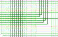
Oops, my bad
You can probably imagine that I didn't really feel like redrawing most of that with nets instead of wires. Just ignore it, I'll fix it someday when I have the time and it won't actually hurt anyone. More importantly are design choices where it turns out I'm not that familiar with electrical designs as I make people believe. For starters, I've never worked with ferrite beads before but it's recommended that the TMS3818 has one in it's power supply. Did I connect it correctly and is this a good choice? I wouldn't know. Also, the digital signals going in and out of the VGA connector are vague. The DDC signals are I2C, but I can't find anywhere if they really have to be 5V. In the end, I added a little voltage level switcher with a MOSFET on those lines. From other schematics I deducted that the hsync and vsync lines (which are only out, naturally) could be simply connected to a 3.3V chip with the addition of a resistor. But again, I'm not sure so help is always welcome here.
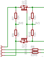
Does this make sense?
Lastly I have no idea how to decouple my power supplies for the FPGA, the CPLD and the SDRAM. I've found a helpful document from xilinx which explaines quite a few things and I've deducted by now that the capacitors I've drawn currently aren't going to be enough. So that needs work before I can start with the circuit board design. Oddly enough I was always taught at school that for decoupling you had to use electrolytic ones, but those are expensive, big and not used by anyone else. Even that document says that ceramic ones are best, which are the most sensitive for noise and might actually produce noise themselves. Weird, but hey, what do I know.
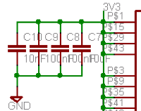
This needs work, since it won't work now
So all in all, I made some serious progress this week (at least, that's how it feels) and hopefully I can finish the board next week. Although I'm not to sure what thickness to use for what wires. If they're too thin, they break when etched and I can't use the circuit board, and if too thick I'll end up with inductance trouble. So yeah, next week will be a blast, even though apparantly I'm supposed to be a week off. Oh well. For everybody who wants to have a peek at the completed schematic, here's a PNG image. Or, if you have Eagle installed, here's a zip file with the schematic and my custom library. Feel free to check both for errors, I'd greatly appreciate it!
[: wacco :]