


 You're on the Project VGA Page


Progress #3
Update 2007/12/13: Early release board artUpdate 2007/12/10: Added talk about fpga<->cpld clock
Posted on 2007/12/07 - 17:15
It has been a hectic few weeks with all kinds of things happening. First, we had quite a few visitors (hi!) which killed the server I was lurking on, so I had to move in no-time. Which took all night. Then at some other point Reinder fixed a new server and we could move back to the old domain but in all this moving around we confused quite a few people so now there are multiple locations people can find us. Whatever. During all that I made some changes to the website to get the layout fixed up for more browsers, so it should work in pretty much anything that's capable of displaying text. And we've got a new, more permanent domain; projectvga.org.
Besides the whole polishing of the website I received lot's of mail and comments telling me this was a cool project and refering me to other projects, help, potential issues, you name it, I received it. And it's damn motivating so keep 'em coming, I love it. I was also asked to write an article for a magazine which will be distributed to a few thousand businesses to promote my university, and in return they will cough up some of the finance needed to cover the costs of the prototype. Great! All this did push back my planned deadlines though because simply 'finishing the circuit board' suddenly became 'find a spare hour'. That makes it all somewhat annoying, knowing that you spend a week doing only organisatorial stuff without getting anything 'constructive' done. Naturally I did get stuff done, but not the stuff I was planning to. So to get that out of my system I worked a bit on some new backend stuff for perennial last week. The idea I had isn't finished yet but is shaping up quite nicely, and I'll work out the details somewhere next year or something.
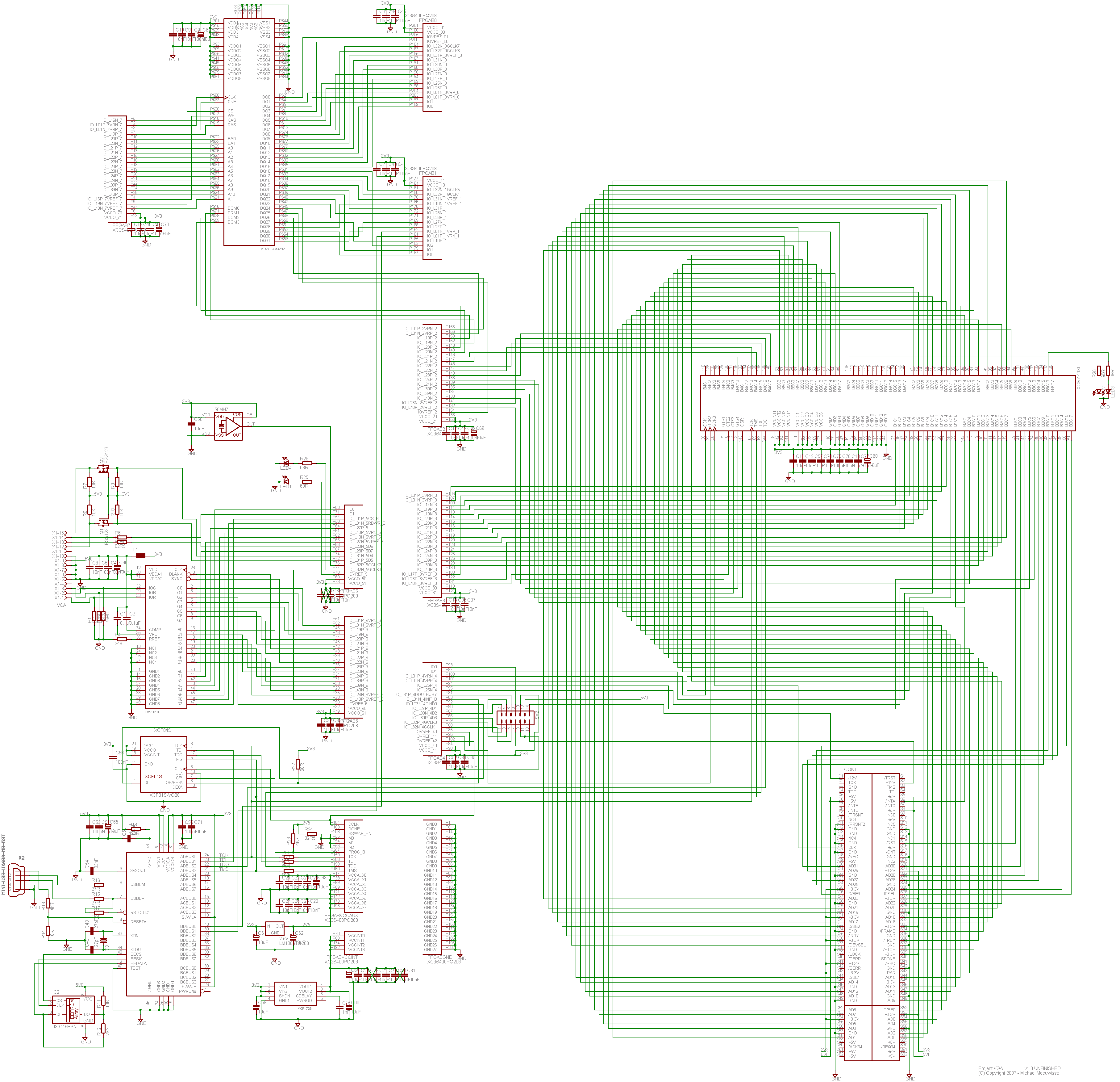
Anyway, yesterday the final components (the FPGAs) arrived, so I'm finishing up the circuit board. The north side of the FPGA and the power lines of the SDRAM still have to be worked out partially, but other than that most of it is done. There are a lot of 'rough edges' however so I'll spend probably most of next week finetuning it all. To give you an idea of what I mean with mostly done, a beta screenshot:
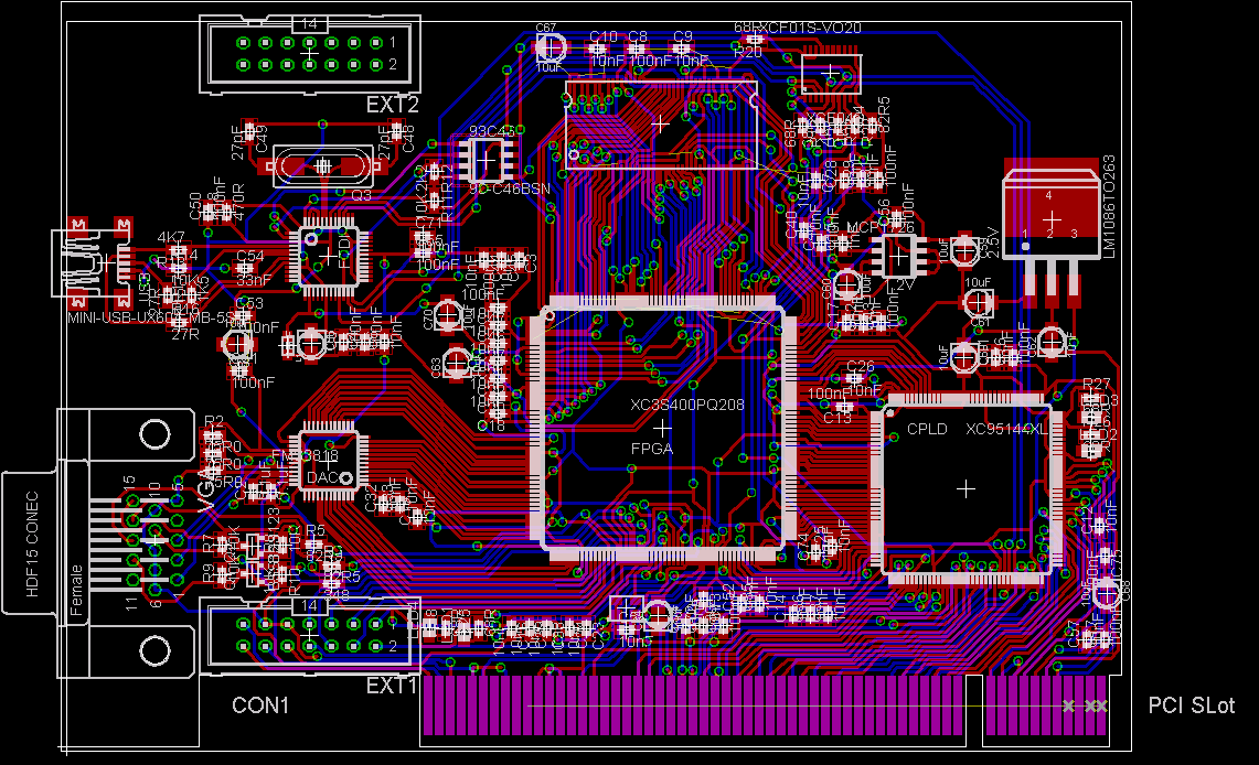
Current progress (click for large)
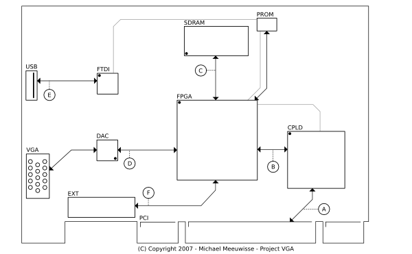
And I actually believe that's all for now. I added EXT2 for any extension cards, which could use some stability after being connected to EXT1. I'll probably keep all those pins unconnected, I *might* route some to the CPLD (just in case somebody says, "I wish you'd done that, then I could've done xyz") but I'm not sure if it's possible. In any case, hang in there, the next post will be the rest of the Modules design which I'll write up sometime soon.
Update 10 dec:
This is important enough to report straight away, but not big enough to create a new entry. I received an email
from André Pouliot and after a few mails he argued:
The clock in that case would use the general
routing inside the chip before connecting to the clock tree. That would
cause a lot of timing problem for the IO on the bridge side of the chip.
In some case you could see some pin captured before or after the
transition giving you erroneous data. Also since it would be using
general routing, after each rebuild the clock would have a different
delay before arriving to the flip-flop.
You can use any pin to output a clock. For receiving it you better use a
GCLK pin. I had once to do it without using a GCLK pin I can tell you it
wasn't fun.
He has an excellent point here, so I changed the schematic in such a way that there's now a signal from the CPLD going to GCLK2 on the FPGA. I took this opportunity to make the interface to the CPLD slightly larger, so I sacrified a LED on the FPGA for this and the bus to the CPLD is now 37 lines wide, with one dedicated clock line. I'll reflect this in the other documentation later. Unfortunately, the placing of the pins on both sides makes the clock line significantly longer than the other lines. But we'll have to deal with that somehow, I can't see any other way at this point.
Update 13 dec:
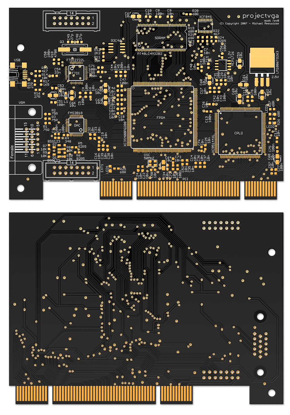
Again I don't feel like writing a full entry. I gave myself the deadline of friday to get the board art finished,
and although I've got one day left I'm mostly finished. I still got to fix some details to get the ground planes
rendered nicely, which is somewhat irreversible so you don't see them here yet. Other than that, I'm good as done!
Except for a final re-check to make absolutely sure that everything is in fact, correct. For your
entertainment:
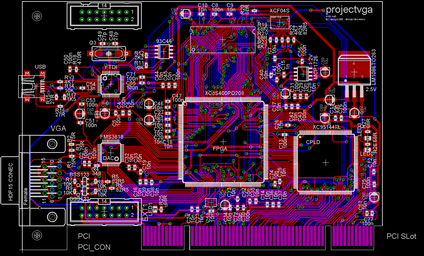
Nearly finished! (click for large)
50+ hours so far just this week. I'm completely beat. This is definitely the last time I'm routing everything by hand. Next time I'll throw more layers at it until it can route it by itself. Or let some other idiot do it. Some changes you might not instantly spot are; PCI connector is now 3.3V compatible, has holes for a bracket, and gold plating is correct. All silkscreen text is now readable and ordered. Over 600 clearance errors (mostly because I turned the minimum clearance way up above what's needed) are removed. All power lines are now thicker. A bunch of capacitors for reducing noise have been relocated. Components and wires surrounding the clocks have been reorganised to reduce any noise, as well as the power lines near the DAC. And finally, a bunch of little changes for aesthetic reasons.
[: wacco :]