Project VGA


project vgaYou're on the Project VGA Page, welcome! Hope you enjoy it!

Schematic


Old:
version 1
version 2
version 3
Current:
image (large)

Board art


Early beta
Prototype
Artist impression (large)
Eagle Files v1.1
Eagle Files v1.2
This zip contains current schematic, board and library.

Diagrams


Block Diagram (SVG)
HDL Modules (SVG)

Places to go


Open Graphics Project
Cadsoft Eagle
Hogeschool van Amsterdam

xhtml 1.0 strict
css
GPL 3.0 License

Wacco Webstack

Module Design

Update 2007/12/28: Added module descriptions, changed talk about bus C.
Posted on 2007/11/18 - 22:57

This is very much a work in progress. Feedback will be appreciated, nothing is definitive yet. This article will expand the moment more details are worked out.

Good news everyone! -- Hubert J. Farnsworth

After lenghty consideration I figured, what the hell, and switched to the GNU General Public License 3.0 so that should at least get a lot of those "You're not really Open Source!" smartasses out of the way. So there. I haven't checked everything yet so you might find BY-NC-SA still somewhere. Let me know if you spot it, I'll remove it at once.

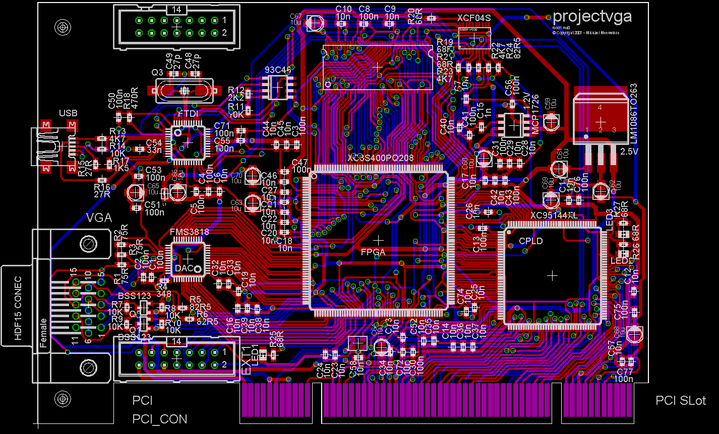
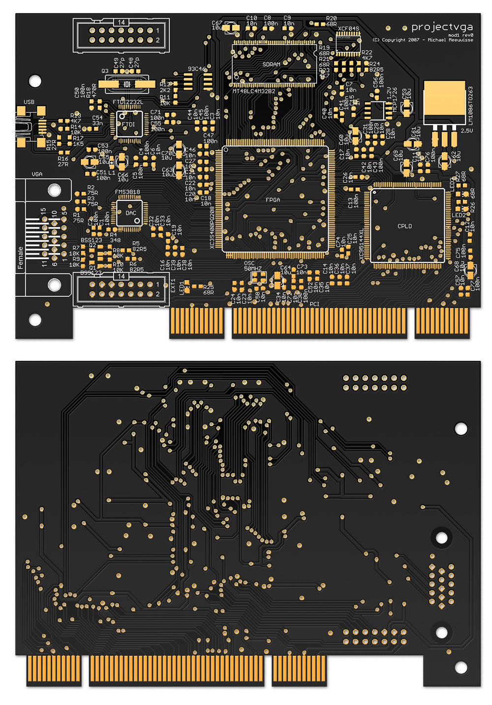
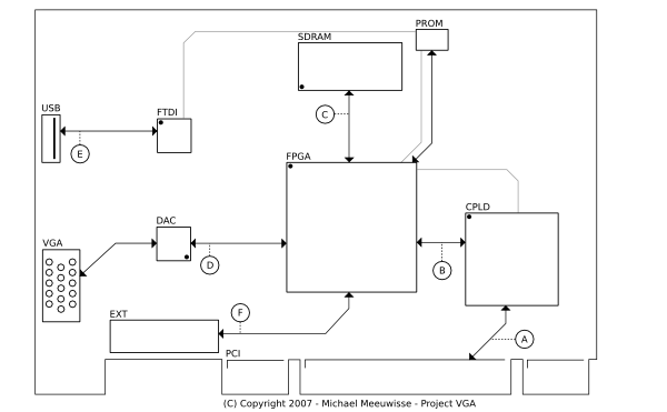
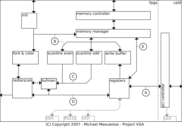
I finally found the time to get accustomed to Inkscape, but only because it got about damn time that I figured out how to use graphics editor. So, if you haven't seen it yet, the talk about communication now has an accompanying Block Diagram to clarify a whole lot of things. This also gave me the possibility to sketch up some doodles I had laying on my desk for a while now, and worked out the module design for the FPGA and CPLD. After about a day work (I didn't say I got fast with inkscape) I ended up with this:


HDL Modules

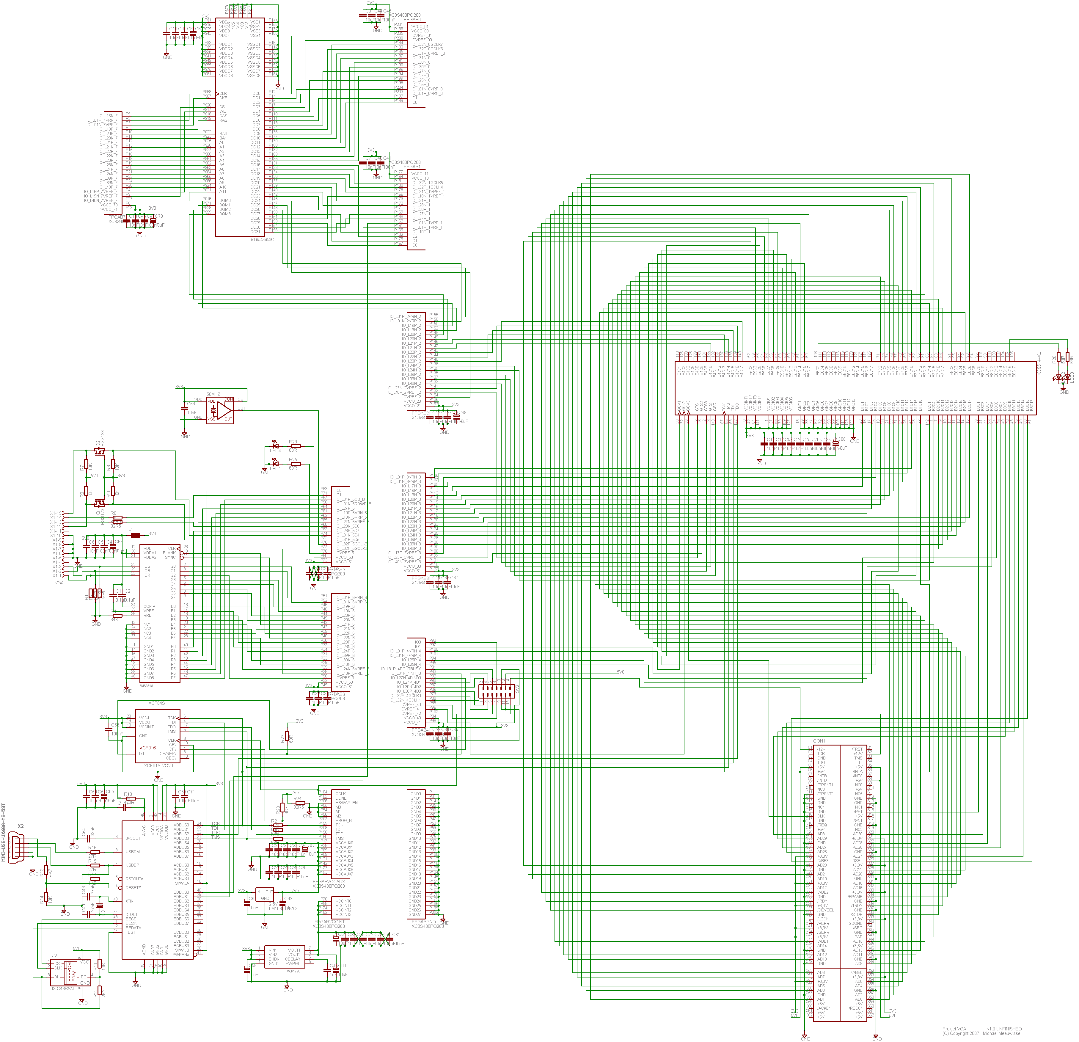
So, right. I figure nobody really wants to read all of this right from the start, so I'll split it up in individual sections which discuss all the components. I'll make a note here that I won't quite discuss the gray areas partly because I haven't worked them out yet, and partly because they're available, but not really used. It's more for extentions, customizations and debugging that these ports are available in the first place. DDC is a notable exception, it's just that I won't really implement this at first. If a bus isn't discussed seperately check the module it's connected to.

A: Bridge bus
This is the bus between the FPGA and the CPLD, so it has some special properties. For one, it's limited to 38 lines and that includes the clock signal. Second, being that it's a physical bus means it won't be as fast as everything else and will probably need some extra buffering. Part of the PCI Controllers' job is to remap the memory space and IO space, so this means there won't be 32 address lines needed. The other bits might be useful for Bus Command singals, however because these are also used as Byte Enable during the data phase of the PCI spec, this might not entirely be possible. Currently it might be possible to have AD[31:0] and C/BE[2:0], CLK, IRDY and TRDY. In this setup, a subset of C/BE[3:0] will be mapped because not all options will have to be implemented by the FPGA. For example, IO and Memory Read/Write can use an address line to indicate what space is used. Frame will be mapped to IRDY meaning the FPGA will always have to be ready for recevining, which isn't unrealistic. With TRDY the FPGA can let the CPLD know it wants to send data, which can then be acknowledged somehow. Lines like IDSEL can be left out since the bus will no longer be shared among devices. In any case, 38 lines will be tricky but not impossible.

B: Memory bus
The memory bus connects the buffers with the Memory Manager. It has a multiplexed address and data bus of 32 bits wide. Control lines like device select are seperate for each buffer and driven by the Memory Manager. During the init phase this bus is used and controlled by the Init module instead. It is bidirectional in the sense that data can go from the buffers to the memory manager and vice versa, but each buffer individually can only be read from or written to by the manager. There's no support for communication between buffers.

C: Cache bus
The cache bus is controlled by the Buffer Manager and provides the Raster Scanner with data. It's 32 bits wide and can be used during retrace periods to put a new address value in a buffer. At all other times, depending on a signal selecting a buffer, the bus contains valid data. This means that the retrace signal from the rasterscan propagates to the buffers as an output enable signal. The buffers auto-advance their internal offsets, so no control signal other than a clock is needed.

A discussion on the Open Graphics mailing list made clear that you don't actually need two buffers for this, since it's in hardware and all the buffers are dual ported. Also, there is already a rasterscanner which has a buffer manager embedded in it available. I'll have to read up on how it works exactly but it's probable that the buffer manager and two scanline buffers will be replaced by some simple glue logic and a single buffer instead.

D: Register bus
The register bus simply directs any register values which are requested or changed to the rasterscan in case they relate to the mode settings. Fonts and colors are redirected to memory, which the Memory Manager then in turn writes to the buffer if needed. Signals like when the Raster Scanner is in a retrace period are send to the Register module. This bus will probably be only 8 bits wide, since the traditional DAC is programmed using 8 bit registers. An few extra signals will indicate for which register the data is currently meant.

E: Direct-Read bus
This bus is here to make it possible to directly reply to PCI requests from memory. The registers module maps incoming addresses directly to the Memory Manager using this bus and can signal the Memory Manager that it needs this data in case the C/BE lines indicate so. The Memory Manager can then instantly send this request to the Memory Controller which will return the data as fast as it can. This data then ends up on the Memory Bus (B) which can be accessed by the Register module through this Direct-Read bus. Because the Memory Manager will be running in a higher clock domain than the Register Module and PCI connection, it's possible to reply directly to read requests. It should be possible to stay below the maximum of 16 clocks after a read started on the PCI bus (see section 3.5.4.1. of the specification) with this setup. Writes are buffered, so a write immediately followed by a read for the same address might cause a race condition. The registers module makes sure this won't happen.

PCI Controller
The PCI Controller listens in on the PCI bus and responds to requests specific for this card. This includes the memory areas of the VGA standard if these are enabled in the appropiate register. If it detects a request it replies and translates the address to a mapping. This in turn is then send to the Register module on the FPGA. Similarly, if the FPGA wants to send something it let's the PCI Controller know which in turn sends this onwards. Note that all requests except PCI related or address translation related registers are send onward to the Register module. The only thing the PCI controller does is filter out the PCI details of the requests.

Registers
The Registers module is called this way due to lack of a better name. It receives requests from the PCI Controller and sends these to the correct module if needed, or stores / retrieves any register that isn't specific to any module in particular. For example, if the output clock is configured, this data is send to the Raster Scanner and not actually stored in the Registers module. If a read request is performed this module uses bus E to interrupt the Memory Manager and retrieve the data from bus B (not shown, considered part of bus E in the illustration). For writes is places this data first in the Write buffer to support longer bursts. Reading is not possible as long as there's data in the write buffer, the register will deny any requests.

Write Buffer
The write buffer is a dual ported fifo which makes it possible to receive write bursts from the PCI controller without having to throttle or interrupt the memory manager. Nothing special here, although the memory manager has to give it a fairly high priority - the registers module can't initiate read requests as long as there's data in this fifo.

Memory Manager & Controller
The Memory Manager has to keep track of all fifos and requests, and prioritise accordingly. It can receive signals from all fifos as soon as they have data to offer or request, and poll for the required address. It then passes this address to the controller which communicates with the actual memory. The controller is given a handle for each request which it will return with the data. The manager uses these handles to determine for which fifo the data was originally destined and pass the data on correctly. The controller can temporarily pause the manager when it's refreshing portions of the memory.

Init
The init module loads all configuration data like default fonts and the pci eprom in memory on startup. It talks directly to the memory manager and can not be ignored by it. Only once the init module finishes loading, the memory manager is allowed to start dealing with the other buffers. During this startup fase, the font & color buffer has top priority, only after that the scanline buffers will be activated.

Scanline even & odd & Buffer Manager
These fifos manage the graphics data to be displayed. It's probably wiser to only implement a single fifo which, due to it's dual port features, can be kept filled while the raster scanner reads from it. The buffer manager issues the required addresses and can be configured by the registers module for other ranges. If we end up using the OGP raster scanner, this is already done by the raster scanner instead and a buffer manager isn't necessary.

Raster Scanner
The raster scanner creates the correct synchronization signals for the vga output and reads from the scanline buffers the visual data. If the scanner is currently in a text mode it does a translation to actual pixel data with help from the font & color buffer. Finally, it sends this to the video output. The raster scanner can be configured by the registers module for which mode it needs to be in.

Font & Color
The font & color buffer holds the font mapping and color palette for all modes requiring these. It can be updated at any time by writes from the memory manager. The memory manager knows what section of the memory the buffer duplicates and will send new data to the buffer if this part is updated. Because of this, the buffer doesn't hold any address related data.

[: wacco :]

Comments


Posted by Gregory_NZL on Sat, 10 Nov 2007 23:40:53
I have high hopes for open hardware. Go for gold!
Posted by BSDfan on Sun, 11 Nov 2007 01:20:36
I hate to break it to you.. but it's not entirely complicated to design a VGA-compatible video card.

In high school, I designed my own 8bit ISA card.. is this group planning on supporting 3D acceleration of any kind?

Please.. how is this at all more impressive then any old 2MB PCI video card?
Posted by NiceGuy on Sun, 11 Nov 2007 03:17:46
Good luck :)

@ BSDfan, ... try not to be a prick about other people's projects :( if your so awesome why don't you go ahead and help them :/
Posted by BSDfan on Sun, 11 Nov 2007 05:26:26
@NiceGuy..

Why? it would be easier just to give everyone an old PCI video card.. I've got a large collection in my basement.

Seriously, This is pointless.. A video card is trivial, a graphics card.. is not.
Posted by Sean on Sun, 11 Nov 2007 08:28:11
The point, BSDFan, is that the card is reprogrammable and the card is an open design. That allows hobbiest developers to do things that are entirely impossible on old PCI video cards (they are not reprogrammable), and those old cards are no longer produced nor are their designs freely available for reproduction by hobbiest board developers.

One might ask, BSDFan, what the heck the point of BSD was since commercial UNIXes already existed.
Posted by Unanimous Cow Herd on Sun, 11 Nov 2007 09:41:33
Some of us STILL ask what the point of BSD is!
Posted by nulleight on Sun, 11 Nov 2007 13:53:23
Yeah, especially now that we have linux already... Anyway i think it's a great project which may have maybe not a great practical but a significant educational value.
Posted by matthews on Sun, 11 Nov 2007 17:44:09
But will it play doom
Posted by matthews on Sun, 11 Nov 2007 17:45:51
ok seriously this is cool great work guys I hope you inspire a generation of hardware designers
Posted by R2 on Sun, 11 Nov 2007 17:57:42
Well, I think this is cool and all, but I've got a question: When you mean "under 200 euros", do you mean it will be SIGNIFICANTLY cheaper, or just 199.00 euros? Because, if its just a little bit cheaper, even 150.00 euros, there's no point to it. I mean, you can get a high-performance radeon x1950 for about that price, and no, it doesn't have 16MB of vram, it has 512MB, and its much more powerful. I understand this is for the sake of open-sourceness, but if its too expensive no one will buy it.
Posted by wacco on Sun, 11 Nov 2007 18:59:46
@BSDFan: If it's not entirely complicated, why does it already take 3 years for the OGP to develop one? The point of this project is to get development /started/ on a usable platform, not to be an /end product/ as a video card. We're certainly aiming for 3D support and all the other graphic spectacular stuff (shaders and whatnot) but that might not come until version 2 or 3 of this card.

@R2: We're keeping some room for mass production costs and stuff. We're not really business people so we don't have a clue. Right now, we're looking at about a 100 euros in components, but then you'd still need to manually assemble it. If we make more cards, that price goes down, but they have to be factory assembled, so price goes up. We simply don't know yet. :)
Posted by Raffaele on Sun, 11 Nov 2007 20:11:30
Wow... Extraordinary. It seems that in the Netherlands there is lots of people talented with hardware and so open minded to release their products with Open Source licenses.

Take a look at Minimig, the Amiga 500 Clone that it is also based on FPGA chip which emulates original Amiga Multimedia Chipset.

http://home.hetnet.nl/~weeren001/minimig.html

http://en.wikipedia.org/wiki/Minimig

Hope that both projects (ProjectVGA and Mimimg) could interact and enhance the capabilitiy of this little beautiful mini-computer...

See also Open Source re-implementation of Minimig with Mini-ITX form factor:

http://web.comhem.se/illuwatar/project_pages/minimig/minimig.htm
Posted by Ignatius Cheese on Sun, 11 Nov 2007 21:40:47
I think this is a really cool project and a great learning exercise. This strategy of starting out with something relatively simple and then expanding on it, is the right way of doing it IMO.

Some commenters seem to think that your first iteration prototype should be able to compete with mass-produced commercial cards with thousands of engineering hours behind them, which is of course absurd.

How many PCB layers are you going for on this board, 4?
Posted by betaluva on Sun, 11 Nov 2007 21:52:46
hi, i posted some info on the reactos website,GreatLord has offered to write a windows driver for your card, heres the link if your interesyed: http://www.reactos.org/forum/viewtopic.php?t=4709
Posted by wacco on Sun, 11 Nov 2007 22:18:58
@Raffaele: That sure is an interesting project, but I don't know those guys. We are however underway with getting some interaction between OGP and us, so soon we'll hopefully grow beyond our little team we have right now.

@Ignatius: Just two right now. It's mayhem to route, but affordable to produce.

@betaluva: Sounds great! However, we'll be plenty busy with implementing plain vanilla VGA support (your good old bios boot screen and 640x480 stuff) which is already supported by all operating systems. Keep in touch, we might need you guys later!
Posted by dmoore on Mon, 12 Nov 2007 02:11:16
A virtualized version of the graphics card would be very useful both to test on and use. Particularly something adaptable to QEMU. The built in graphics card emulator for QEMU is fairly weak but might be worth dissecting.
Posted by master on Mon, 12 Nov 2007 06:29:57
por que tan caro??, quien carajo les va a comprar, si quieren tener exito debe costar alrededor de 100 dólares.

he dicho...!!!
Posted by 6205 on Mon, 12 Nov 2007 07:27:41
Nice bullshit...
Posted by Isaac on Mon, 12 Nov 2007 08:32:55
I think that this is fantastic. I believe in the vision, the effort and the methods, and I would likely purchase a card even if it had only decent 2D support, for the principle. If it was Voodoo3 3000-level, that'd be incredibly sweet, but I can still upgrade through two or three versions until something like that happens. (^^) Good show and best of luck!
Posted by canci on Mon, 12 Nov 2007 09:46:42
Wow! This is a great effort! Wish I had money spare to support you, but, alas, I'm just a poor student from a developing country... the kind of guy who'd definetly benefit from such hardware. With various free *NIX clones and a, hopefuly, soon open bios, the future looks great!
Posted by nn on Mon, 12 Nov 2007 13:03:09
xxx
Posted by VMSfan on Mon, 12 Nov 2007 16:47:49
What is the point of this? I made a Cray XMP emulator on my ZX80 in my sleep when I was an infant (that was faster than the original), and that was soo easy. That makes me much better then you! (Now, if only I could be smart enough not to post meaningless crap to usefull websites...)
Posted by translator on Mon, 12 Nov 2007 17:26:48
Here is a translation of what the Spanish guy says:
"Why so expensive? Who the f*** will buy it, if you want to be successfull, it must cost around 100 dollars"
My take: If you don't even have the courage to post in English so that others can read your BS, then don't critize others who have the courage to go and start something new.
Posted by Daniel Cabrini Hauagge on Mon, 12 Nov 2007 22:04:51
Very nice project!

Just a comment on the "porting the designs to gEDA" part. Have you looked at KiCAD? It's also opensource and in my opinion much easeir to use and feature rich.

http://www.lis.inpg.fr/realise_au_lis/kicad/
Posted by wacco on Tue, 13 Nov 2007 19:39:03
Due to heavy traffic (not that I mind!) we ran out of bandwidth and the site is now temporarily hosted on a server of the Hogeschool van Amsterdam. That's why you'll get a 302 redir if you attempt to access the mveas.com address.
Posted by Henry Keultjes on Wed, 14 Nov 2007 16:10:28
Anyone watching what's going on with LinuxBIOS?
Posted by todthgie on Wed, 14 Nov 2007 22:15:14
yep i am ... im a bit active in both projects i have LB almost running on an old Netier and im working on a Compaq Deskpro SFF right now ... almost finished
Posted by Ignatius Cheese on Thu, 15 Nov 2007 20:02:19
Hi again Wacco. Just a few small pointers that you may be aware of already.

With only two layers, you have to take good care to get proper grounding everywhere, otherwise your card won't work well. It's easier with 4, cause then you can have a one inside layer as a dedicated ground plane.

I'm not so sure about your level shifting circuit with FET:s. First, I don't understand how it's supposed to work. Second, even if it works, FET:s are capacitive so you will get a quite slow circuit I think. Maybe you should make an experiment, put together the components and try it out?
Posted by wacco on Thu, 15 Nov 2007 22:12:04
I'm aware of the ground plane being a bit of an issue and the card will probably have some noise issues on higher frequencies (I'm a little worried about the SDRAM connection) so I'll be careful not to have 'floating' planes anywhere.

The level shifting thing is indeed a little odd, I grabbed it from the following site:
http://delphys.net/d.holmes/hardware/levelshift.html which mentiones:
http://wwwasic.kip.uni-heidelberg.de/lhcb/Publications/external/AN97055.pdf
It might be a good idea to test it first, I should have enough components for that anyway. I'll fix up a little circuit next week. If it wouldn't work; what would you replace it with?
Posted by Ignatius Cheese on Sat, 17 Nov 2007 00:30:46
Had a look at the sites you referred to. Very clever solution I must say. It looks like it works at quite high speeds too (~1MHz). The only concern is, can an FPGA pin sink enough current to make this work properly?

For possible alternatives, you could take a look at the LTC4300A-2 buffer from Linear. It seems to do the job though I haven't tried it myself, it costs a tiny bit more and it's not quite as fun as the FET solution..
Posted by wacco on Sat, 17 Nov 2007 02:59:55
On the spartan 3 you can specify the IO pins being LVTTL (that is, 3.3V IO) and specify a 'maximum current drive' attribute of 24mA. I figure this would be for pulling a pin up, and I'm assuming it'll be capable of pulling at least the same amount down. With the 10K resistor, we're talking about less than half a mA (If I'm making correct calculations at this time of day..) so I think that'll work without a problem.
Oh, and don't bother about the speed, it's an I2C connection for the DDC data, and the FPGA is the master, so it doesn't matter much since we can clock it really slow if we really have too.
Thanks for checking! :)
Posted by Froilan Squirtle on Wed, 21 Nov 2007 01:34:32
Hi again!
I dunno if you have received my comment on your FAQ...
I'm a programmer, I love game programming, and I know a bunch about Opengl, allegro and a little SDL, so if you need something just tell me ;)
I dunno anything about electronics (well almost anything) but I find this project to be quite interesting, and I've always wanted to learn a little about electronics and everything, and thats a (big) start! :p

Keep up the good work!
Posted by areYou SureItsMe:) on Fri, 11 Jan 2008 04:02:07
hey compadre,
looking good let me know when we can toast to succes!!
you know who
Posted by wacco on Sat, 12 Jan 2008 20:08:51
Yo! You've got yourself a deal ;)
Posted by michael a. beaver on Sat, 19 Jan 2008 01:07:05
A totally VGA compliant and fast 2D video card is not a trivial matter. In fact, there are still a number of folks selling verilog source IP for this on the internet.
http://intrinsix.com/intrinsix-ip/vga/vga-core.htm
Just to educate the unwashed masses. Their are a number of books on the market which may help with this effort:
1) Programmers's Guide to EGA, VGA, and Super VGA cards by Ferraro
2) The PC Graphics Handbook by Julio Sanchez and Maria P. Canton
To support compliance testing I would recommend the following folks:
http://elpin.com
This is the web site of Elpin Systems. They have been doing VGA compliance testing since the 1980s.
I am waiting for one of you to actually post a block diagram of a VGA compliant graphics device complete with a CRT controller, cursor controller, attribute controller, etc. (Hint: start with the IBM 6845 CRT controller as a starting point).
Posted by Electron9 on Mon, 21 Jan 2008 01:41:14
A suggestion is to use XC3S500E, it have a larger logic array. You'r not likely to use the obscure I/O modes that XC3S400 offers. But is likely to have use for the extra logic capacity.
I think the hard stuff will be:
1) SDRAM interface
2) PCI handling concurrent to framebuffer scanning.
3) Any possible electrical issues (maybe #1 ?).
I didn't find any HDL code..?, I prefer verilog btw :)
You may want to protect your VGA I/O with BAV99 dualdiodes. Video ports are prone to blowing up..
As for the BSD Bashers, the point of BSD is stable and tidy code. And in particular code mature before inclusion.
Posted by wacco on Wed, 23 Jan 2008 17:14:50
@Michael beaver,
Very interesting to see and thanks for the pointers. I'll have a look those books. And yeah I know, the HDL modules design is wrong in a few points and misses some things, but I'm in the middle of this semesters' exams so I've got no time to update it.
@Electron9,
It's a little late to switch to the S500E but it's definitely on the wish list for the next version. Especially because we can swap the S500E out with the S1200E for people who want to go even bigger. I'll have a look at those diodes you mentioned.
As far as I know nobody has actually started on the HDL code yet, we'll be going for verilog but some other stuff is more important at the moment. Stay tuned. :)
Posted by Electron9 on Thu, 24 Jan 2008 06:52:14
Yeah XC3S500E (PQ208) was a suggestion for next revision. Another optimisation that might be worthwhile is to put the SDRAM closer to the connector side. Such that the FPGA chip can be put higher up. And thus leave more room for routing.
Don't forgett that most computers bootup in 720x400 @ 70 Hz.
Posted by louis vuitton on Tue, 15 Jun 2010 12:21:21
see, I'm having 3x 8 bits, plus a clock and some sync lines going from the FPGA to the DAC. You'd have to do something similar for a DVI chip. If you want something like this, I suggest you start your own project!
The tg68 project is really nice, I hadn't heard of that yet. If it fits (including the rest of minimig) on a xc3s400, then yes, minimig will probably run on this card.
Posted by chanel bags on Wed, 14 Jul 2010 04:47:36
FAST shipping, item exactly as described! I'll shop again.|mire101
Fantastic Item, can't wait to see more from you|bianka2009
love the bags, great buy and very nice seller, hope to do more transactions!|kimdeguzman
Posted by chanel bags on Wed, 14 Jul 2010 04:56:32
i love the bags, it was beautiful, nice seller, highly recommended!|kimdeguzman
as described; quick postage - excellent transaction|goslara
Very pleased with item. Fast shipping. Recommended seller. Thank you.|keekspurses
Posted by chanel sale on Wed, 14 Jul 2010 04:57:14
I LOVE my dream bag, smooth transaction, great communication with the seller!|opinionatedms
Amazing!!! Exactly as it was described. Fast shipping. Thank you seller!!!|megmariem1982
Beutifull bag. Fast shipment.|maschen84
Posted by Designer handbags on Fri, 06 Aug 2010 13:31:55
Designer handbags and Louis Vuitton Replica Bags many style, 24/7 live service!
Posted by mbt shoes on Fri, 13 Aug 2010 11:38:15
huang101niceboy
Posted by herve leger on Fri, 13 Aug 2010 11:39:18
haveagirl
huang101
Posted by louis vuitton bags on Fri, 13 Aug 2010 11:39:49
goodday
huang101
Posted by youmarco66 on Fri, 27 Aug 2010 10:49:00
nice blog!
Posted by ecco shoes on Fri, 27 Aug 2010 11:00:22
nice blog@
Posted by sdfdsf on Sat, 04 Sep 2010 09:58:54
<a href=http://www.chanelearrings.org/fake-Replica-Bracelet-83-b0.html>replica cartier bracelet</a> Frequent or unexplained switches in <a href=http://www.chanelearrings.org/fake-Tiffany-Bracelets-30-b0.html>tiffany bracelets</a> plan managers can be a <a href=http://www.chanelearrings.org/fake-Links-Jewelry-37-b0.html>piddly links jewelry</a> tip off.
Posted by With so many people struggling <a href=http://www.chanelearrings.org/fake-Bvlgari-Ring-125-b0.html>bvlgari ring</a> financially b on Sat, 04 Sep 2010 10:00:05
GOOD
Posted by Click on the <a href=http://www.chanelearrings.org/fake-Links-Charms-45-b0.html>links charm</a> highlighte on Sat, 04 Sep 2010 10:00:59
good
Posted by botsfan on Wed, 08 Sep 2010 09:27:25
Thanks for sharing!

Leave a comment